
Figure 15 A top view of a metamaterial inspired switch having a DGS and secondary switches in accordance with an aspect of the new structure.
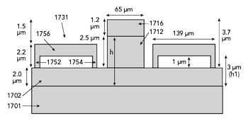
Figure 16 Side view of the switch shown in Figure 15.
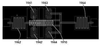
Figure 17 Example layout of the metamaterial inspired MEMS switch.1
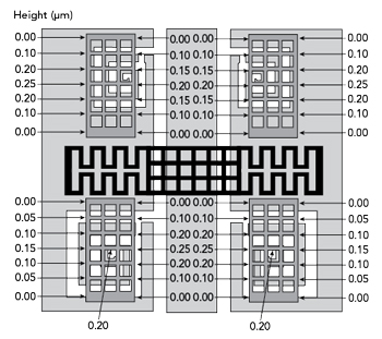
Figure 18 The amount of downward deflection at several points of the secondary switches (measured in μm) when the secondary switches are actuated.1
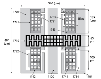
An example MEMS shunt switch with DGS structures and overlaid secondary switches is shown in complete form in Figure 15, which includes a signal line 1720 positioned between a first ground plane 1702 and a second ground plane 1704, the signal line separated from each ground plane by first and second spaces 1703, 1705, respectively. A primary shunt switch 1710 is positioned on top of, is connected to and bridges the first and second ground planes 1702, 1704. The primary shunt switch 1710 runs perpendicular to, and is suspended over, the signal line 1720. When a bias voltage is applied to the primary shunt switch 1710, the switch 1710 deflects downward toward the signal line 1720. When the bias voltage is not applied, the switch 1710 deflects back upward to its original position.
A first DGS structure 1731 and a second DGS structure 1732 are formed in the first ground plane 1702. A third DGS structure 1733 and a fourth DGS structure 1734 are formed in the second ground plane 1704. The first and third DGS structures 1731, 1733 have mirror symmetry along a lengthwise x-axis of the primary switch 1710 and are a similar shape. The second and fourth DGS structures 1732, 1734 also have mirror symmetry along a lengthwise x-axis of the primary switch 1710 and are a similar shape.
In the example of Figure 15, the first and third DGS structures 1731, 1733 are a different size from the second and fourth DGS structures 1732, 1734. The second slots of the first and third DGS structures 1731, 1733 are about 85 μm long, whereas the second slots of the second and fourth DGS structures 1732, 1734 are about 100 μm long. The third slots of the first and third DGS structures 1731, 1733 are also shorter than those of the second and fourth DGS structures 1732, 1734. This contrasts with the four DGS structures shown in each of Figures 7 and 10, which all have the same dimensions.
Each DGS structure is overlaid by a respective secondary shunt switch 1741, 1742, 1743, 1744. Each secondary shunt switch is connected to its respective ground line and is suspended over its respective DGS structure with an air gap in between. The secondary shunt switches are rectangular, each of the secondary switches positioned lengthwise parallel to the signal line 1720 and perpendicular to the primary shunt switch 1710. The secondary switches positioned above the first DGS structure 1731 and the third DGS structure 1733 have a mirror symmetry with the secondary switches positioned above the second DGS structure 1732 and the fourth DGS structure 1734 along a lengthwise x-axis of the primary switch 1710. Additionally, the secondary switches positioned above the first DGS structure 1731 and the second DGS structure 1732 have a mirror symmetry with the secondary switches positioned above the third DGS structure 1733 and the fourth DGS structure 1734 along a lengthwise y-axis of the signal line 1720. The secondary shunt switches 1741, 1742, 1743, 1744 are also perforated. In the example of Figure 15, the switches have a grid-like lattice perforation.
Figure 16 shows a side-view of the switch of Figure 15. The switch in Figure 15 is formed on a substrate 1701. A ground plane 1702 is formed over the substrate 1701, and the primary switch 1710 is formed on top of the ground plane 1702. The primary switch 1710 has two feet 1712 (the second foot is obstructed by foot 1712 in Figure 17) supporting a beam 1716. Two secondary switches 1731, 1732 are positioned on either side of the primary switch 1710. Each of the secondary switches also includes two feet 1752, 1754 supporting a beam 1756. DGS structures (not shown) are formed in the ground plane 1702 at respective positions underneath the secondary switches 1731, 1732.
In the example of Figures 15 and 16, the substrate and ground planes have a length of about 404 μm, and a width of about 340 μm. The ground planes have a thickness of about 2 μm. The primary switch 1710 extends the length of the substrate, the primary switch feet 1712 and beam 1716 have a width of about 65 μm. The feet 1712 have a height of about 2.5 μm, and the beam 1716 has a thickness of about 1.2 μm. The secondary switches 1731 have a length of about 139 μm, and the secondary switch feet 1752, 1754 and beam 1756 have a width of about 65 μm. The feet 1752 have a height of about 1 μm, and the beam 1756 has a thickness of about 1.2 μm. Thus, the entire switch in Figure 15 can be formed on top of the substrate 1701 within a 5.7 μm space.
New Metamaterial MEMS Switch
Figure 17 shows an example layout of a metamaterial inspired MEMS switch, showing the connections between the primary switch 1910 and secondary switches 1941-1944, a first actuator 1962 and a second actuator 1964. The first actuator 1962 is connected to the primary switch 1910 and configured to provide a bias voltage to the primary switch. The second actuator 1964 is connected to each of the secondary switches 1941-1944 and is configured to provide a bias voltage to the secondary switches.
In operation, the primary switch shown in Figure 17 may be either ON (bias voltage provided from the first actuator 1962) or OFF (no bias voltage provided by the first actuator 1964). When the primary switch is ON, the primary switch beam deflects downward, resulting in a large shunt capacitance that blocks RF signals from propagating along the signal line 1920. When the primary switch is OFF, the primary switch beam deflects back upward (at rest), reducing the shunt capacitance and permitting RF signals to propagate along the signal line 1920.
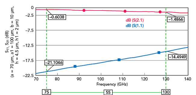
Figure 19 Plot of return loss and insertion loss of the switch described in Figure 17 with the secondary switches activated.
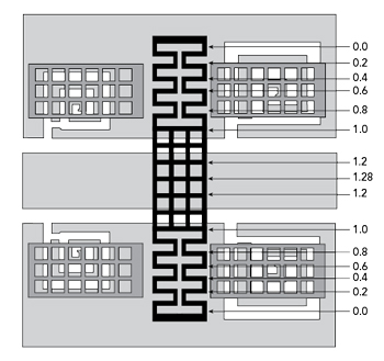
Figure 20 The amount of downward deflection at several cross-sections of the primary switches (measured in μm).
When the primary switch 1910 is OFF, the secondary switches 1941-1944 may be turned ON in order to negate the effects of the DGS structures toward insertion and return loss. A bias voltage is applied from the second actuator 1964 to each of the secondary switches 1941-1944, thereby causing the switches to deflect downward toward the DGS structures and create a shunt capacitance blocking the effects of the DGS structure.
Figure 18 shows the amount of downward deflection at several points of the secondary switches (measured in μm) when the secondary switches are actuated. Figure 19 shows return loss and insertion loss characteristics for the MEMS switch illustrated in Figure 17 when the primary switch is OFF, and the secondary switches are ON. At 75 GHz, insertion loss is as low as about 0.6 dB and return loss is as low as about 21.1 dB. At 130 GHz, insertion loss is still relatively low at about 1.5 dB, and return loss is also relatively low at 14.5 dB. Returning to Figure 17, when the primary switch 1910 is ON, the secondary switches 1941-1944 may be turned OFF in order to get the benefit of the DGS structures toward isolation. No bias voltage is applied from the second actuator to the secondary switches 1941-1944, so the switches remain separated from the DGS structures underneath by the airgap.
Figure 20 shows the amount of downward deflection at several cross-sections of the primary switches (measured in μm) when the primary switch is actuated. Deflection along the entire width of the primary switch is uniform for any given point along the length of the switch.
Figures 21 and 22 show the isolation characteristics for the MEMS switch in Figure 17 when the primary switch is ON and the secondary switches are OFF. In Figure 21, the same DGS structure is used. This leads to a significant improvement in isolation at a relatively narrow band (e.g., less than about 10 GHz, between 90 and 100 GHz). At 75 GHz isolation is about -23.1 dB and at 130 GHz, isolation is about -23.9 dB. But at about 95 GHz, isolation is improved to about -52 dB.
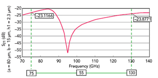
Figure 21 The isolation characteristics of the switch of Figure 17 having varying air gap heights.
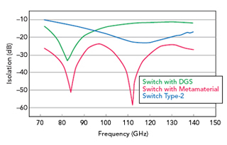
Figure 22 Isolation characteristics for switches with different topologies.
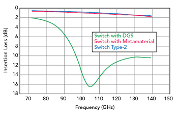
Figure 23 Insertion loss characteristics for switches with different topologies.
Figures 22 and 23 show plots of isolation and insertion loss characteristics for MEMS switch utilizing different structures. The metamaterial construction leads to an overall improvement of isolation over a wider band of frequencies. The structure represented in Figure 15 yields improved isolation at about 84 GHz (about -51 dB) and at about 112 GHz (about -59 dB) and is not worse than about -24 dB between 75 and 130 GHz. The insertion loss characteristics of the DGS switch is poor compared to the regular switch and metamaterial versions. Switch Type 2 is the first version of the new MEMS Switch using Capacitive Contacts.
As seen from the attenuation characteristics of Figures 19 and 21, providing DGS structures with capacitive MEMS shunt switches above the DGS structures is an effective way of incorporating the benefits of DGS for improved isolation when RF signals are blocked, while at the same time negating the detriments caused by the DGS to insertion loss and return loss when RF signals are propagating. In this respect, incorporation of DGS structures and corresponding shunt switches are an improvement to RF MEMS design and operation. Table 1 provides a summary of the actuation voltage, isolation and insertion loss characteristics for the above-described switch designs with air gaps (and cantilever beam heights) of about 2.5 μm.1
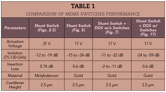
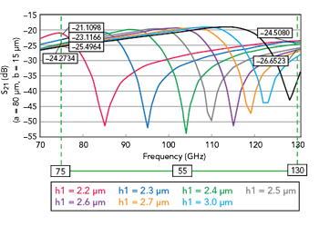
Figure 24 Isolation characteristics for various MEMS switch designs.
Figure 24 shows isolation characteristics for several switches having different DGS and secondary switch arrangements, in which both switches are actuated. Actuating the secondary switch results in improved isolation characteristics over a narrow band of frequencies. The band at which the improved isolation occurs varies depending on the air gap height between the switches and DGS structures. As the air gap increases, the frequency band at which the best isolation for the switch occurs shifts upward. For an air gap of 2.2 μm, isolation of about -52 dB is achieved at about 85 GHz and for an air gap of 3.0 μm isolation of about -44 dB is achieved at about 122 GHz. This demonstrates the relative flexibility of the proposed combination of DGS structures with secondary switches for providing improved isolation across a wide range of high frequencies.
Conclusion
In Part I of this three-part series, it is shown that both the DGS structures and secondary switches can achieve improvements in insertion loss and isolation. These improvements contrast with the tradeoffs conventionally seen when using either only a shunt switch (good insertion loss, poor isolation) or only a DGS structure (improved isolation, but worse insertion loss). The proposed combination of a primary shunt switch, DGS structures and secondary shunt switches is shown to behave like a metamaterial. In addition to this solution, it also improves resistance to stiction of the MEMS switch using metamaterial layers within the design of the switch contacts which will be covered in detail in Parts II and III.
References
- Shiban Koul, Ajay Poddar and Ulrich Rohde, “Microelectromechanical Switch with Metamaterial Contacts,” US Patent Pub. No. 02161415A1.
- Astrid Lambrecht, “The Casimir Effect: a Force from Nothing,”Physics World, September 2002.
- F. Intravaia and C. Henkel, New Frontiers of Casimir Force Conference, Santa Fe, New Mexico, 2009.
- U. Leonhardt and T. G. Philbin, “Quantum Levitation by Left-Handed Metamaterials,” New J. of Physics, August 2007.
- Mercado et. al.,“A Mechanical Approach to Overcome RF MEMS Switch Stiction Problem,” ECTC 2003.
- Chaitanya Mahajan, “Design and Analysis of RF MEMS Switches (70 GHz to 130 GHz), M.Tech dissertaion, CARE, IIT Delhi, May 2018.