
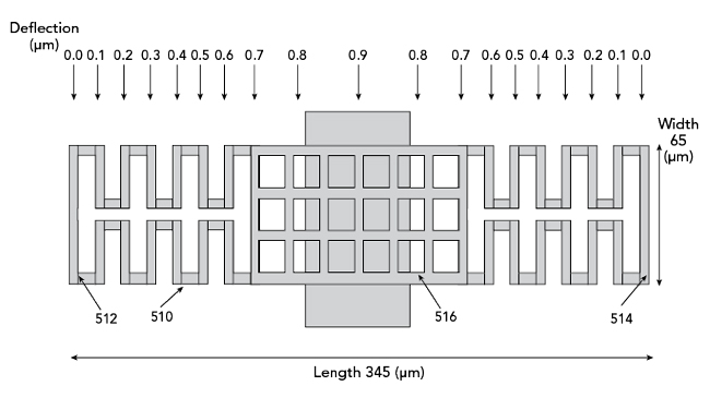
Figure 5 Plan-View of capacitive shunt switch using a serpentine structure in the cantilever beam.
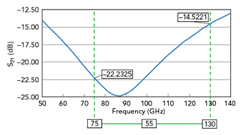
Figure 6 Shows the isolation plot of MEMS shunt switch in Figure 5.
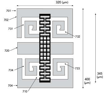
Figure 7 Shows the Plan-View of the DGS inspired MEMS switch.
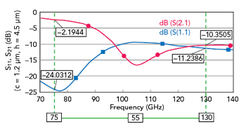
Figure 8 Shows the return loss and insertion loss of MEMS switch in Figure 7.
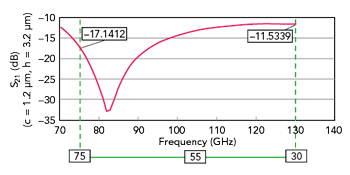
Figure 9 Shows the isolation of MEMS switch in Figure 7.
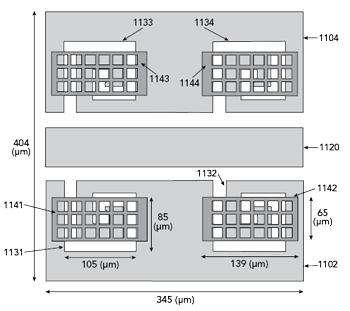
Figure 10 Shows the Plan-View of a switch, secondary MEMS switches are placed above the DGS.
In the example of Figure 5, the MEMS switch includes a rectangular beam 510 made of gold and having a perforated structure. The middle portion 516 of the beam 510 forms a perforated grid or lattice. Each corner of the lattice structure then extends in a serpentine pattern toward the first and second ends 512, 514 of the beam 510. The serpentine patterns on either end are then connected to one another, thereby forming first and second serpentine structures on either end of the beam 510. The serpentine structure permits for deflection of the beam with a lower bias voltage. The dimensions of the switch shown in Figure 5 are largely comparable to that of Figure 3 except that the beam of Figure 5 is slightly longer (about 345 μm), and slightly wider (about 65 μm). The beam still deflects downward up to 0.9 μm but with only a 17 V bias voltage. The MEMS switch of Figure 5 exhibits improved isolation characteristics.
Figure 6 shows isolation characteristics of the switch of Figure 5 when the switch is open, across the 75 to 130 GHz band. Isolation is about -22 dB at 75 GHz, about -14.7 dB at 130 GHz and drops to as little as about -24.8 dB at 86 GHz. Insertion loss of the switch when closed is only about 0.6 dB and return loss is about 15.15 dB.
New DGS Capacitive MEMS Switch
The isolation characteristics of these new shunt switches can be further improved by incorporating DGS, particularly in the mmWave frequency band of 75 to 130 GHz. A two-dimensional DGS is formed in each of the ground planes 702 and 704 of the MEMS switch shown in Figure 7. The DGS essentially behaves as a band stop filter, thereby affecting the transmission characteristics of the switch. Figure 7 includes a beam 710 having the same structural arrangement as the beam 510 of Figure 5 and formed on a ground plane structure 701 measuring about 320 μm long by about 400 μm wide. The ground plane structure 701 includes a signal line 720 between two ground planes 702, 704. In the example of Figure 7, the DGS forms four spiral shaped slots 731, 732, 733, 734 in a two-by-two grid and having mirror symmetry along the lengthwise axis of the signal line 720. Each of the spiral shaped slots have a common, uniform width.
Figure 8 shows insertion loss and return loss of the switch in Figure 7 when the switch is closed. The typical insertion loss is 2.2 dB at 75 GHz and 10.4 dB at 130 GHz, but drops as low as 16.6 dB at 105 GHz. Return loss is about 24 dB at 75 GHz and about 11.2 dB at 130 GHz but increases to about 9.5 dB at 105 GHz. Figure 9 shows isolation for the DGS inspired MEMS switch illustrated in Figure 7 when the switch is open. Isolation is about -17.1 dB at 75 GHz and about -11.5 at 130 GHz and drops as far as about -32.5 dB at 82 GHz. Although isolation characteristics of the switch of Figure 7 show improvement, higher insertion loss limits the applications. To overcome the insertion loss, variation to the DGS structures are incorporated to Figure 10.
The MEMS switch shown in Figure 10 is similar in structure to that of Figure 7. As illustrated in Figure 10, the MEMS switch has two ground planes 1102, 1104 bisected by a signal line 1120 and has four DGS structures 1131, 1132, 1133 and 1134 formed in the ground planes. The length of the ground planes and signal line are about 340 μm, and the cumulative width of the switch is about 404 μm. MEMS switch as shown in Figure 10 differs from Figure 7 in that each of the DGS structures includes a secondary MEMS switch 1141, 1142, 1143, 1144 positioned above the DGS structure. The shape of both the secondary switch and DGS may be rectangular, but the secondary switch may be longer while the DGS structure may be wider. In the example of Figure 10, each DGS structure is a perforated lattice, and is about 105 μm in length and about 85 μm in width, overlaid by a secondary switch that is about 139 μm in length and 65 μm in width. The MEMS switch described in Figure 10 includes a substrate 1101 on which the ground plane is formed. The ground plane has a thickness or height of about 2 μm.
Although not shown, the slots of the DGS structure 1131 are formed in the ground plane and may have a depth equal to the height of the ground plane 1102. A secondary switch 1141 is formed above the DGS structure 1131. As depicted in Figure 10, the secondary switch 1141 includes a beam 1151 supported by two feet 1162, 1164. The supporting feet have a height of about 1 μm, thereby raising the beam 1151 about 1 μm above the DGS and ground plane. Thus, there is an air gap of about 1 μm between the non-deflected beam and the DGS positioned below. The beam thickness or height of the beam 1151 may be about 1.2 μm.
The beam 1151 shown in Figure 10 is connected to an actuator (not shown) to supply a bias voltage, which runs from the beam 1151 to the ground plane 1102 via the feet 1162, 1164. Applying the bias voltage causes the beam 1151 to deflect downward toward the ground plane 1102, thereby affecting the capacitive characteristics of the DGS structure 1131. The amount of voltage applied to the switch 1101 may be continuously variable and thus the capacitive characteristics of the DGS structure (and its effect on the main MEMS switch of the device) can be varied or tuned.
It has been found that the switch arrangement of Figure 10 behaves like a metamaterial (engineered material). This can be seen by first analyzing the transmission and reflection phases of a signal line formed in a coplanar waveguide without the DGS structure of Figure 10, and then analyzing the transmission and reflection phases of the same signal line with the DGS structure of Figure 10.
For a simple coplanar line without DGS, the transmission and reflection phase are analyzed. The results are shown in Figure 11; the transmission and reflection phases of a signal transmitted across a coplanar waveguide without the DGS structure over a band of mmWave frequencies from 50 to 140 GHz. As shown, any shift in the transmission phase of the signal is met with a substantially equal (within about 20 degrees) shift in the reflection phase.
Figure 12 shows transmission and reflection phases of a signal over the same band of frequencies for the same coplanar waveguide but with the DGS structure incorporated into the waveguide at a height of 2.2 μm, which is the distance from the top surface of the substrate (the basin of the slots of the DGS structure) to the bottom surface of the secondary switch positioned above the DGS structure. The transmission and reflection phases do not shift equally across the band of frequencies, and even shift in opposite directions, eventually crossing one another at 85 GHz and then crossing back at 96 GHz.
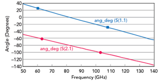
Figure 11 Transmission and reflection phase for the coplanar line of a switch without DGS.
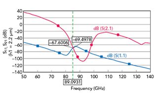
Figure 12 Plots of the transmission and reflection phase for the coplanar waveguide with DGS in Figure 10 for a height 2.2 μm.
Figure 13 shows transmission and reflection phases for the same coplanar waveguide but with the DGS structure at a height of 2.8 μm. The transmission and reflection phases shift substantially equally until about 110 GHz, but then begin shifting in opposite directions at frequencies above 115 GHz and even cross one another at about 128 GHz. The resonance frequency of the DGS structure thus varies depending on the height of the air gap between the ground plane and the beam.
Figure 14 shows a plot of isolation characteristics for five secondary switches positioned over DGS structures at varying heights. The resonant frequency of the structure is shown to shift to higher frequencies as the air gap between the ground plane and beam increases.
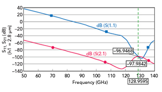
Figure 13 Plots of the transmission and reflection phase for the coplanar waveguide with DGS in Figure 10 for a height 2.8 μm.
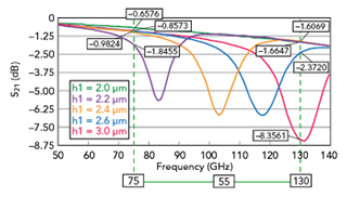
Figure 14 Plots of isolation characteristics for five secondary switches positioned over DGS structures at varying heights.