
Editor’s Note: This article is based on US Patent Application No. 62/469,752, March 10, 2017. It describes a new micro-electromechanical-system (MEMS) switch technology in a three-part article over the next three issues. Part I reports on MEMS switch topologies including a new defective ground structure (DGS) and metamaterial inspired capacitive contact MEMS switch; Part II reports methods to reduce stiction effects in a resistive contact MEMS switch; and Part III discusses methods to reduce static friction (or stiction) effects in a capacitive contact MEMS switch for applications in modern electronic circuits and 5G communications.
A new MEMS switch with improved isolation, insertion loss and reduced liability for stiction is reported for the applications in high frequency electronics and communication systems. MEMS switches are suitable for signal routing for transmit and receive applications, switched line phase shifters for phased array antennas, wide band tuning networks and high precision instrumentation applications. Typical MEMS switches are categorized by the contact methods, capacitive (metal-insulator-metal) and resistive (metal-to-metal).
MEMS switches are typically a silicon-based integrated circuit technology with moving mechanical parts that are released by means of etching sacrificial silicon dioxide layers. MEMS switches include a signal line having an input port and output port between first and second ground planes, and a beam for controlling the activation. In this article, the variation of the switch architecture includes one or more DGS formed in the first and second ground planes, and a corresponding secondary deflectable beam positioned over each DGS. For reducing the vulnerability of stiction, the switch incorporates an artificial engineering structure known as metamaterial for creating the repulsive Casimir interactions to mitigate the stiction related issues in switches.1-6
Compared with PIN diodes or field effect transistor switches, MEMS switches offer lower cost and improved performance (power consumption, isolation, insertion loss and linearity). However, MEMS switches can encounter several drawbacks: high actuation voltages, high insertion loss and poor return loss. In addition to this, MEMS switches are susceptible to electromechanical failure after many switching cycles, especially under hot switching conditions. For instance, the switch may fail due to stiction buildup. When the moveable part of the switch is pulled into contact with another component of the system (e.g., a signal line); the static friction can cause the switch to become stuck and non-functional. It may require a high voltage to overcome the stiction force. But at low voltage, the switch can remain “welded” to the component.
MEMS Switches
MEMS switches are usually categorized by the contact methods: capacitive (metal-insulator-metal) and resistive (metal-to-metal). Capacitive switches use a thin layer of dielectric material to separate two conducting electrodes when actuated. The dielectric layer prevents direct metal-to-metal contact. Therefore, stiction of contacts due to thermal energy is less of a concern. However, the thin layer of dielectric material will only conduct signals with reasonable insertion loss when the coupling between conductor electrodes is above a certain frequency. Moreover, the isolation bandwidth of capacitive switches is limited by the ratio between the ON and OFF capacitances. Metal-to-metal switches use physical contact of metal with low contact resistance to achieve low insertion loss when actuated. Therefore, the metal-to-metal MEMS switches can be operated from DC to RF frequency with isolation defined by the coupling capacitance of the electrodes when the switch is open. The metal-to-metal contact is made by surface asperities and the true contact area is much smaller than the apparent contact area. For the metal-to-metal contact to have low contact resistance, some plastic deformation of the asperities is required.
In general, as the pull-down force increases, the asperity deformation increases and the contact resistance decreases. However, adhesion of the contact point is proportional to the contact area and the temperature associated with the degree of deformation, so lower contact resistance is often accompanied with stronger adhesion. RF switches carry RF signals, so in certain operation conditions, such as impedance mismatch, a high level of RF power will pass through the switches. In such cases, the heat generated by RF power may cause micro-melting of asperities and could potentially short the contact points.
Before the integration of metal-to-metal switches into 5G mmWave communication systems become a reality, the adhesion (stiction) problem and reliability associated with the contacts needs to be resolved. The possible techniques for reducing the surface adhesion is either by selecting contact materials with less adhesion by applying chemical surface treatment or eliminating contamination with plasma cleaning.
Figure 1 illustrates a typical example of a cantilevered out-of-plane MEMS switch. Figure 1a is a cross-sectional view of the switch along X-axis; Figure 1b is a top view of the switch; and Figure 1c is a cross-sectional view of the switch along Y-axis. The typical MEMS switch is formed over a coplanar waveguide 101 in which a signal line 110 is formed between ground planes 102, 104 on a substrate 105 as shown in Figure 1. The signal line 110 includes an input port 112 and an output port 114 formed on opposing ends of the substrate 105. The cantilever switch includes a post 120 or anchor affixed to the substrate 105 and includes an extension extending over the substrate in a direction perpendicular to the signal line 110. The extension of the cantilever includes a bottom layer 125 of dielectric material, such as silicate and a top layer of conductive material 130, such as gold. The cantilever further includes a contact bump or dimple 135 positioned underneath the bottom dielectric layer 120 and in alignment with the signal line ports 112, 114. Thus, when the cantilever is bent downward, the dimple 135 contacts the signal line 110, thereby connecting the input and output ports 112, 114.

Figure 1 A typical MEMS switch: (a) cross-sectional view along X-axis, (b) top view and (c) cross-sectional view along Y-axis.
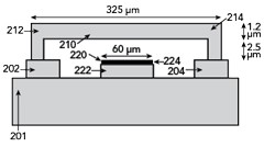
Figure 2 Shows Side-View of switch using a doubly supported cantilever beam designed above a coplanar waveguide.
In addition to this, the MEMS switch depicted in Figure 1 also includes an electrostatic actuator (not shown) for actuating the cantilever by applying or removing a DC bias voltage between the cantilever and the ground 102, 104 of the coplanar waveguide 101. The cantilever bends downward and upward, in a direction toward and away from the signal line, respectively, in response to the applied voltage from the actuator. Other RF MEMS switches may rely on a lateral movement in order to bring the moveable part of a cantilevered switch toward or away from a contact. Each moving part and contact may be metal (resistive switch), or one may be metal while the other is dielectric (capacitive switch).
New MEMS Switch using Capacitive Contacts (Metal-Insulator-Metal)
Figures 2 and 3 show the side view and top view of capacitive contacts shunt MEMS switch with a doubly supported cantilever beam 210 formed above a coplanar waveguide formed on a substrate 201. As shown in Figure 2, the first end 212 and second end 214 of the beam 210 are supported by respective ground planes 202 and 204 formed in the coplanar waveguide. The middle of the beam 210 is suspended over a signal line 220 formed in the coplanar waveguide. The beam 210 is connected to an actuator (not shown) configured to apply a DC bias voltage across the beam 210 and the ground planes 202, 204. The DC bias voltage causes the beam 210 to deflect downward. The signal line 220 includes a conductive layer 222 covered by a thin dielectric layer 224, such as silicon nitride.
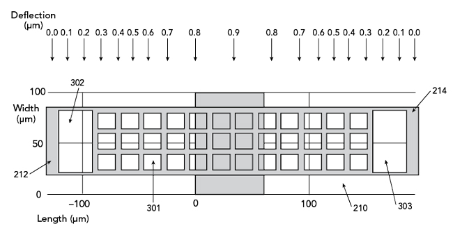
Figure 3 Shows the Plan-View of switch with a doubly supported cantilever beam above a coplanar waveguide.
The dielectric layer is selected about 0.2 μm thick. When the beam 210 deflects downward and contacts the signal line 220, a large shunt capacitance is obtained. The large shunt capacitance blocks RF signals from propagating along the signal line 220 of the coplanar waveguide (ON-state). When the DC bias is removed, the beam 220 deflects upward and returns to its original position, the shunt capacitance drops and the RF signal resumes propagating in unattenuated form (OFF-state).
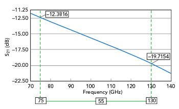
Figure 4 Shows the isolation plot of MEMS switch depicted in Figures 2 and 3.
In Figure 2, the beam 210 is made of molybdenum, and has a length of about 325 μm, a width of about 60 μm and a thickness of about 1.2 μm. The signal line 220 extends through the coplanar waveguide and has a width (in the direction of the beam length) of about 60 μm. The beam 210 is suspended about 2.5 μm above the signal line 220, thereby forming a 2.5 μm air gap. The dielectric layer has a thickness of about 0.2 μm.
As shown in Figure 3, the beam 210 is perforated, having a grid of small perforations 301 in the middle and a large perforation 302, 303 at each end. The perforations yield improved downward deflection of the beam 210. It can be seen that vertical displacement of the beam 210 when the DC bias voltage is applied, which extends from no displacement at the respective ends 212, 214 of the beam, to about 0.91 μm in the middle of the beam 210. The DC bias for the switch has been observed to be about 37 V.
Figure 4 shows the plot of the isolation characteristics of the switch in Figure 2 when the switch is open, across a band of mmWave signals from 75 to 130 GHz. The typical isolation is about -12.4 dB at 75 GHz, and about -19.7 dB at 130 GHz. The typical insertion loss of the switch when closed is about 0.74 dB and return loss is about 10.04 dB. The actuation voltage needed for the switch can be further reduced by providing a different perforation arrangement.