
Figure 8 compares the transistor power performance and output third-order intercept (OIP3) for both the PP15-6x and PP15-5x processes, measured at 29 GHz and 6 V VDS. PP15-6x has 1 dB more gain, 10 points higher PAE and increased Psat. The 29 GHz OIP3, measured with a two-tone input signal separated by 10 MHz and using the optimal input and output impedances, shows this latest generation achieves an OIP3 improvement of 2 to 3 dB relative to PP15-5x.
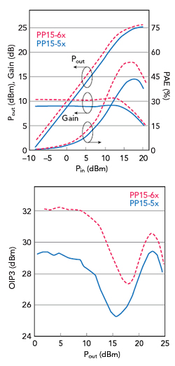
Figure 8 29 GHz swept power and OIP3 for PP15-6x and PP15-5x PHEMT processes.
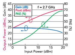
Figure 9 Swept power and efficiency at 2.7 GHz for a 1 mm NP45-11 GaN HEMT.
GaN FOR HIGHEST POWER DENSITY
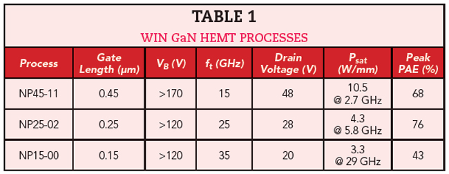
The continued market demand for higher RF power spurred the development and adoption of GaN HEMTs, which deliver impressive RF power and are the principal PA technology where the highest power density and PAE are primary requirements. To support PA designs from 1 to >30 GHz, WIN has developed three GaN processes manufactured on 100 mm SiC substrates, to provide maximum thermal dissipation (see Table 1).
With a bandgap of 3.39 eV, GaN HEMTs have considerably higher breakdown (VB) and operating voltages compared to GaAs, with a bandgap of 1.34 eV. GaN HEMTs also use a source-coupled field plate to reduce the peak electric field and improve breakdown. The field plate enables GaN transistors to operate at drain biases from 20 to >48 V. Fundamentally, the material properties of GaN enable transistor designs with high electron density, and the field plate contributes to the high breakdown and operating voltages to achieve power densities >10 W/mm. Figure 9 shows the 2.7 GHz swept power characteristics of a 4 x 250 μm GaN HEMT from the NP45-11 process. This 1 mm transistor delivers a saturated output power >10 W with 68 percent PAE.
FUNCTIONALITY, FLEXIBLE INTEGRATION
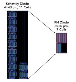
Figure 10 Size of Schottky and PIN diode ESD protection circuits.
To reduce chip counts and simplify assembly, multifunction technologies with functionality beyond the core amplifier are being adopted. Since every MMIC is designed to meet a unique set of requirements, WIN Semiconductors has developed a portfolio of added functions that can be used when needed. These on-chip functions enable electrostatic discharge (ESD) protection, control of PA performance, interface with external control signals or integration of receive low noise amplifiers (LNA) and T/R switches to realize a single-chip front-end.
Perhaps the most basic function is ESD protection. Because of historical process limitations, PHEMT technologies have used large area Schottky diodes for ESD protection. These diodes, which use the same Schottky contact as the PHEMT gate electrode, are limited to approximately 800 V protection using the human body model (HBM). Depending on the level of protection required, these large area diodes can use substantial chip area. To reduce the size, WIN Semiconductors has incorporated monolithic PN junction diodes into its PHEMT processes. They provide up to 3 kV HBM protection and are much smaller than a Schottky, reducing the area by some 80 percent (see Figure 10).
The same process used for PN diodes can be used for PIN diodes. When integrated with a PHEMT process, PIN diodes can provide ESD protection, a power limiter for an LNA or a mmWave T/R switch in a single-chip front-end. Figure 11 shows the measured insertion loss and isolation for two shunt PIN diodes from the PIH1-10 mmWave PHEMT platform. 7 x 7 and 10 x 10 μm diodes have insertion losses of 0.6 and 0.9 dB, respectively.
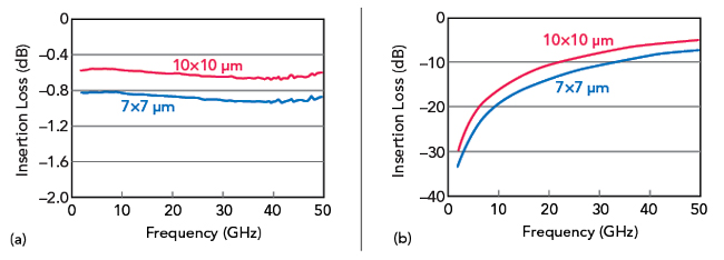
Figure 11 PIN diode insertion loss (a) and isolation (b) vs. frequency.
Figure 12 Two-bit GaAs decoder.
On-chip logic is particularly important for active antenna arrays, to simplify the interface with the beamformer IC. A growing library of logic cells, such as the two-bit decoder shown in Figure 12, has been incorporated into the baseline PIH1-10 technology as process options, to be used if required by the application. These libraries of logic and ESD reference circuits provide designers enhanced tools to add functionality to high performance mmWave front-ends.
Depending on the III-V device used, PHEMT or GaN HEMT, a power transistor can be used as a low noise amplifier or an RF switch. Although adding on-chip functionality, it will entail a performance compromise: an on-chip LNA or RF switch built with a transistor optimized for power density may not have best-in-class noise figure or insertion loss. Nonetheless, it may be a favorable trade-off, by reducing RF losses, parts count or by simplifying assembly and lowering cost. To help designers understand the tradeoffs, WIN Semiconductors characterizes its GaAs PHEMT and GaN HEMT technologies for LNA and switch performance, incorporating models into the PDKs. Design versatility is enhanced by offering optional enhancement/depletion transistors, for logic and digital bias control, and PN or PIN diodes, for ESD protection, input limiting and power switching. These options offer multiple solutions for designing complex circuits and achieving challenging specifications.
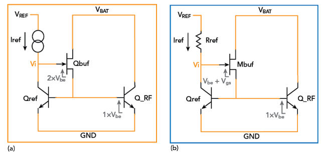
Figure 13 Stand-alone HBT (a) and BiHEMT (b).
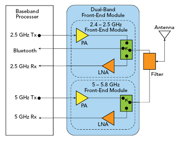
Figure 14 Wi-Fi module using a single-chip BiHEMT front-end.
With GaAs HBT MMICs, increasing the functionality is achieved by adding enhancement/depletion mode PHEMT devices to the HBT process. This functionality is available with WIN’s BiHEMT (bipolar + HEMT) platform. Combining both technologies on the same MMIC provides a high linearity and efficient HBT PA, low loss D-mode PHEMT switch and low Fmin E-mode LNA with control logic. BiHEMT control logic operates at lower voltage, enabling the Venable control voltage to be reduced from 1.2 V, for the HBT process, to 0.75 V for the depletion mode PHEMT (see Figure 13). The integration advantages of the BiHEMT process have been demonstrated by the market’s adoption of single-chip front-end modules for Wi-Fi, which integrate the LNA, switch and PA (see Figure 14). Single-chip front-ends now comprise between 30 and 50 percent of mobile Wi-Fi production volumes.
As mobile devices become thinner, interior board space is increasingly valuable, driving the front-end supply chain to smaller packages - or no package. Similarly, losing 1 dB of power to packaging in a mmWave phased array is expensive. These packaging challenges flow down to the front-end semiconductor technology, and WIN Semiconductors has responded with a portfolio of flexible Cu pillar bump assembly interfaces that minimize package footprint and reduce mmWave losses. Cu bumps are particularly useful for GaAs HBT and BiHEMT technologies, as they form RF/DC connections and provide an improved thermal environment for the transistors in the PA (see Figure 15). The cross-section shows a copper redistribution layer (RDL) used to form high-Q inductors or to position a bump input/output (I/O) above the underlying circuitry. To implement this packaging capability, WIN Semiconductors has internal Cu pillar bump facilities co-located with its wafer fabs.
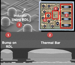
Figure 15 Cu bumps used for I/O, thermal management and high Q inductors.
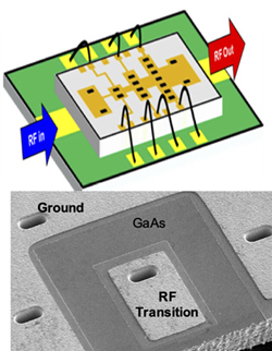
Figure 16 Patterned ground plane for through-chip RF transitions.
At the 28 to 39 GHz bands now being used for 5G links, over-designing the power and LNA to offset package losses is expensive, and the problem becomes more severe at the higher bands used for high capacity wireless backhaul (71 to 86 and 92 to 114 GHz). Bond wire inductances can impair PA performance by >1 dB. I/O bumps at these frequencies are feasible; however, to use them, designs must shift from microstrip to coplanar waveguide. Unfortunately, the industry has limited experience with coplanar design, prompting WIN to develop a process technology to pattern the backside ground plane to isolate the input/output ports and create through-chip RF transitions (see Figure 16). A MMIC design uses microstrip on the topside, with through-chip transitions on the RF I/O ports and standard wire bonds for DC connections. The ground plane is removed on the backside of the RF transition for the I/O connections. The design rules for this patterning technique are flexible; when coupled with a compatible board design and die bonding process, the approach can eliminate RF bond wires from the assembly.
SUMMARY
Compound semiconductors have evolved from performance-driven to the “best value” front-end technology for smartphones, wireless networks and multi-market applications. III-Vs, particularly GaAs, have become the preferred front-end solution, combining best available performance with a flexible amplifier trade-space. This characteristic enables a simpler path to satisfy difficult MMIC performance requirements. With multiple degrees of freedom to optimize and advance transistor capabilities, GaAs and GaN have demonstrated decades of RF, microwave and mmWave performance improvement. These technologies now offer increased on-chip functionality and advanced integration options to support diverse packaging environments, applications and systems.
Over the last 20 years, the annual market for GaAs components has grown to over $9 billion. This expansion has come despite the challenges of increasingly difficult specifications and unrelenting competition from advanced Si processes. As the industry’s leading pure-play III-V wafer foundry, WIN Semiconductors has responded with sustained technology advancement, operational excellence and manufacturing scale. This capability is WIN Semiconductors’ core strength and underpins the continued growth of the GaAs and GaN component market.