
Substrate integrated waveguide (SIW) is useful for the propagation of electromagnetic radiation. It inherits the merits of planar transmission lines such as compactness, low weight, planar nature and ease of fabrication and as well as the merits of metallic waveguides such as minimum loss and maximum power handling capability. The following is a review of SIW technology, a design example and a discussion of key characteristics.
mmWave technologies for 5G, 77 GHz automotive radar and 60 GHz gigabit Wi-Fi require waveguide capable efficient transmission. Microstrip and coplanar waveguide can enable desirable form factors, but do not provide ideal performance. Metallic waveguide can operate efficiently at these frequencies; however, waveguide is large, costly, multidimensional in nature and cannot be easily integrated with planar transmission lines.
SIW offers an effective middle ground. In 1998, SIW capable of transmitting electromagnetic waves was developed.1-2 SIW is a member of the substrate integrated circuit (SIC) family,3 consisting of substrate integrated slab waveguide (SISW) and substrate integrated non-radiating dielectric (SINRD). SICs are useful for high frequency electronics. SIW is also referred to as post wall waveguide or laminated waveguide. It can be fabricated using PCB technology, low temperature co-fired ceramic (LTCC) technology and photo imaging processes. Along with small size and weight, SIW retains the desirable loss and power handling properties of conventional metallic waveguide. It is used as a transmission medium in high speed circuits, antennas, couplers and dividers.4
SIW supports the TE mode of propagation. The absence of TM modes and its inherit structural flexibility makes it promising for filter design. Planar transmission lines such as microstrip or stripline achieve quality factors from 50 to 100, whereas metallic waveguide is in the range of 1000 to 12,000. SIW aims to achieve the intermediate values.5-6
SIW Design
Width
SIW is synthesized by embedding two rows of metallic vias on a dielectric substrate with top and bottom metal claddings (see Figure 1).7 Via holes short both the top and bottom copper claddings so that a vertical current path exists. The propagation characteristics of SIW are almost the same as traditional waveguide.8
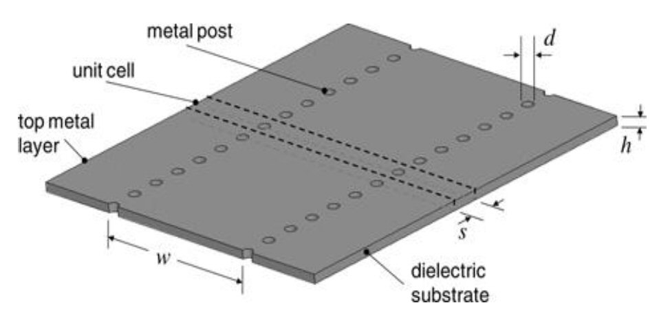
The relationship between SIW parameters and the effective width of rectangular waveguide with same propagation characteristics is:9
weff = w – d2 /0.95 s (1)
where w is the physical SIW width, d is the diameter of the via hole, s is the center-to-center distance between adjacent vias (pitch) and weff is the effective SIW width.
SIW width w is obtained from Equation 1 once the effective width is calculated using Equation 2, where c is the velocity of light, fc is the cutoff frequency of the dominant TE10 mode and εr is the substrate permittivity.
weff = c / (2fc sqrt (εr)) (2)
Equation 1 does not take the effect of d/w into account. Hence, a more accurate relationship is:10
weff = w − 1.08 d2 / s + 0.1 d2/w (3)
Another empirical relation based on the method of lines (MOL) is:11
weff = w × (ξ1 + ξ2/(s / d +(ξ1 + ξ2 − ξ3))/(ξ3 − ξ1)) (4)
Where:
ξ1 = 1.0198 + (0.3465/ (w / s − 1.0684)) (5)
ξ2 = − 0.1183 + (1.2729/ (w / s − 1.2010)) (6)
ξ3 = − 1.0082 + (0.9163/ (w / s+ 0.2152)) (7)
Vias
The design parameters of the via holes must satisfy the conditions:12
d < λg/5 (8)
s < 2d (9)
The pitch must be as small as possible to minimize radiation leakage. To eliminate band gap effect and ensure mechanical rigidity the SIW should satisfy:9
0.05 < s / λc < 0.25 (10)
SIW Parameters
SIW impedance Z0, can be computed from:
Z0 = (h / weff) (η / sqrt (1− (λ/ λc)2) (11)
where free space wavelength and cutoff wavelength are denoted by λ and λc respectively, and:
η = 120π / sqrt (εr) (12)
The phase constant β is calculated for a low loss tangent dielectric material:
β = sqrt [(2πf sqrt (εr)/300)2 – (π/ weff)2] (13)
Here, frequency f is represented in GHz and effective width weff in mm.