
Figure 2 shows a photograph of the four-channel PA die, which measures just under 3.4 mm x 3.4 mm. Its pad positions are like those shown in Figure 1, although the layout incorporates several ground pads to make the circuit testable using on-wafer probes.
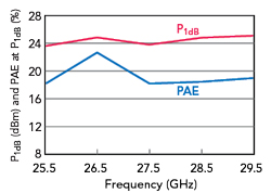
Figure 6 Measured P1dB and associated PAE.
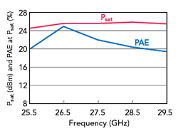
Figure 7 Measured Psat and associated PAE.
SINGLE-CHANNEL MEASURED PERFORMANCE
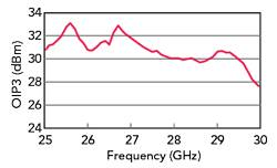
Figure 8 Measured OIP3.
Samples of SMT-packaged PAs were assembled on evaluation boards (see Figure 3), which were designed using a low-cost laminate material suitable for mass production. The single-channel measurements described in this section were performed at room temperature on channel 2 of a typical device, biased at +4 V and a quiescent current density of 100 mA/mm. The measured performance was calibrated to the package pins and includes the IC to PCB transition. A TRL calibration tile was designed to calibrate the measured data to the reference planes of the package.
Figure 4 shows the measured S-parameters of channel 2 of a packaged PA mounted to the evaluation board. The gain was 19.6 ±1.4 dB across 26 to 29 GHz, and the |S11| and |S22| were approximately 10 dB across the band. Figure 5 compares the measured gain with the simulation, where the simulated performance includes an electromagnetic simulation of all the matching networks. Although the PAs for 5G systems will be backed off to operate in the linear region and preserve modulation fidelity, the output power at 1 dB gain compression (P1dB) was measured to provide a figure of merit for comparison. The power and associated power-added efficiency (PAE) are plotted versus frequency in Figure 6. The typical P1dB is around 24.5 dBm, with a corresponding PAE of approximately 19.5 percent. Figure 7 shows the measured Psat and corresponding PAE, which are typically 25.5 dBm and 21.5 percent, respectively.
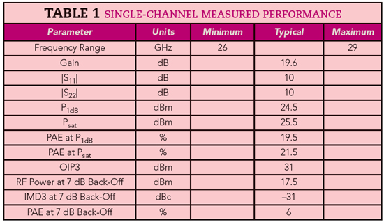
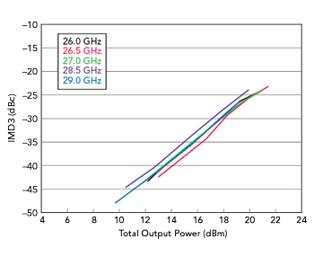
Figure 9 Measured IMD3 vs. total output power at several frequencies.
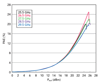
Figure 10 Measured PAE vs. output power at several frequencies.
To reflect the wide channel bandwidths anticipated for 5G systems, the output third-order intercept point (OIP3) was evaluated using a tone spacing of 100 MHz. The measured OIP3 is plotted in Figure 8 at an output power of +8 dBm per tone. The OIP3 is around +31 dBm average from 26 to 29 GHz. Third-order intermodulation distortion (IMD3) versus total output power was also measured at several frequencies (see Figure 9). At an operating point of +17.5 dBm, corresponding to 7 dB back-off, the corresponding IMD3 is −30 dBc or better across the band. Drive-up curves showing PAE versus total RF output power were also measured at several frequencies (see Figure 10). At a +17.5 dBm operating point, 7 dB back-off, the PAE is at least 6 percent across the band.
The on-chip power detector generates a DC voltage to enable monitoring the RF output power. Figure 11 shows the temperature compensated detector output in mV, plotted on a logarithmic scale, versus the RF output power at 27.5 GHz. Over an 18 dB range, the voltage versus dBm characteristic is linear, which simplifies power monitoring.
Table 1 summarizes the measured performance of the single-channel packaged PA.
4-CHANNEL PERFORMANCE
If the four PAs are driven with coherent RF signals and used to drive a four-element antenna array, the RF output signals will combine to provide a 6 dB increase in RF power, i.e., 10log10(N), where N is the number of elements. By appropriately setting the phases of the signals to the four antenna elements, the direction of the antenna beam can be electronically steered. Table 2 indicates the performance that can be achieved from an ideal four-element array, excluding output routing losses and assuming the PAs have identical performance. The table does not include the gain of the antenna elements, which will add to the total effective radiated isotropic power (EIRP), further increasing those parameters specified in dBm in the table.
SUMMARY AND CONCLUSIONS
The four-channel PA MMIC described in this article offers a compelling solution for 5G terminals requiring multiple power amplifiers. The IC demonstrates good performance from 26 to 29 GHz, making it suitable for the full 28 GHz 5G band. To measure and adjust the power, a temperature compensated output power detector is included on all channels.
Fabricated with a 0.15 µm enhancement-mode GaAs PHEMT process, the PA is straightforward to bias and monitor using commercial multi-channel DACs and ADCs. The IC is housed in a compact, low-cost, 5 mm x 5 mm plastic overmolded QFN SMT package, compatible with high volume, low-cost terminals.
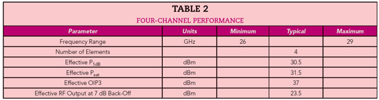
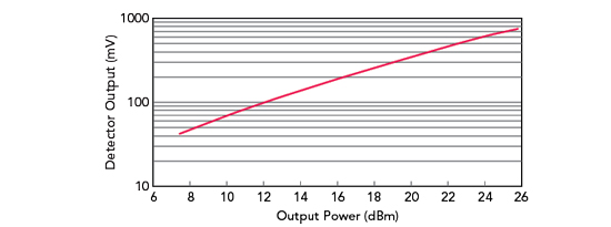
Figure 11 Output voltage vs. RF power for the on-chip power detector at 27.5 GHz.
__________________________________________________________________________
For further information on this subject, Liam Devlin presents on the same topic at the recent ARMMS RF & Microwave Conference. https://youtu.be/yfqkx-GfS1I