
The 1.35 mm connector was created in response to the need for a robust mechanical connector for commercial opportunities up to E-Band, such as satellite and mobile communications and automotive.
Moore’s Law was named after Gordon Moore, cofounder of Intel. In 1965, Moore observed that the number of transistors in a dense integrated circuit doubled about every year. By 1975, the industry unofficially dubbed this Moore’s Law, and Moore modified his prediction to state the doubling would occur every two years.
A similar, less formalized axiom in the world of connectors is a relationship to frequency. In the early 1960s, the 14 mm precision connector was developed to operate to 8.5 GHz, followed by a succession of connector designs to reach higher frequencies: 7 mm, precision Type N, 3.50 mm, 2.92 mm, 2.40 mm, 1.85 mm and 1.00 mm. A loose corollary to Moore’s Law was a 20 to 30 percent increase in frequency with each new connector design. The final leap between the 1.85 mm connector, with a maximum frequency of 65 GHz, to the 1.00 mm connector, with a maximum frequency of 110 GHz and encompassing both E- and W-Bands, is a 70 percent increase in frequency. This double band jump left an opening for a connector for E-Band. Twenty years later when the 1.00 mm connector was commercialized and some deficiencies were realized, the characteristics and design of the 1.35 mm connector was conceived.
Technological innovations are typically driven by research or a commercial application and a corresponding industry supplier. For 1.00 mm connectors, the supplier was Hewlett-Packard, and the connector was formally proposed as a standard (IEEE Std 287-2007) in 1989. However, the first commercial quantities of 1.00 mm connectors were not available until 2010. At higher frequencies, physics constrains the implementation of features such as captivation and connector thread pitch, and the size associated with these higher frequencies results in the 1.00 mm connector being less rugged. Initially, this was not a problem, since the users comprised mostly research facilities that understood how to handle sensitive connectors and cable assemblies.
With deregulation of these frequency bands and applications becoming more cost effective, the commercial world has begun to realize the potential. A group of commercial applications, namely automotive and satellite/mobile communications, reside below 90 GHz in E-Band, and they require large numbers of assemblies that must also be rugged and cost effective. In 2014, SPINNER GmbH decided these applications would benefit from a rugged connector with some but not all of the W-Band connector attributes. Leveraging V- and W-Band connector design features, SPINNER began developing a 1.35 mm E-Band connector with the more rugged construction of the V connector and broadband performance to at least 90 GHz. SPINNER teamed with Physikalisch-Technische Bundesanstalt, the national metrological institute of Germany; Rosenberger; and Rohde & Schwarz to define and develop the 1.35 mm interface. The resulting design was proposed to the IEEE P287 committee, a group revising the IEEE Std 287-2007 for precision coaxial connectors, which decided to include the 1.35 mm connector in the next edition of the standard. In parallel, the interface design was also submitted to IEC, which will publish it as IEC 61169-65.
1.35 mm Connector Design
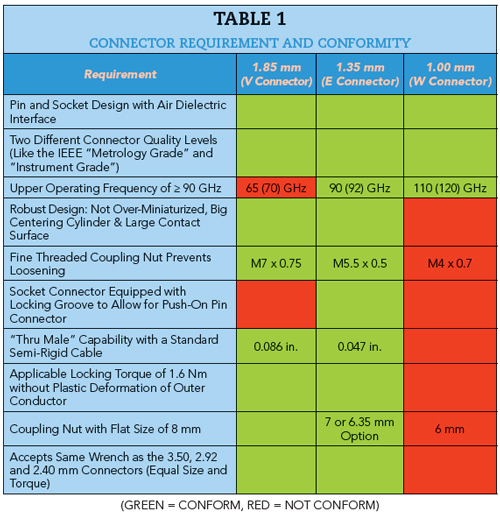
For the 1.35 mm connector interface, several development requirements were defined and realized (see Table 1). The table shows the requirements, comparing them with the other two existing connectors (1.85 mm and 1.00 mm) covering the adjacent frequency bands. Tables 2 and 3 are extracts from the 1.35 mm connector’s electrical and mechanical interface specifications, respectively. The complete specifications and all drawings will be published in the next edition of the IEEE Standard.
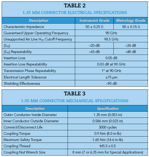
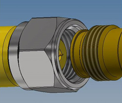
Figure 1 1.35 mm connector pin and socket.
A 3D view of the 1.35 mm interface is shown in Figures 1 and 2. The overall design avoids any unnecessary over-miniaturization, making it strong and robust, even for a frequently used front panel connector on a test instrument. The pin connector features a relatively large centering sleeve (3.5 mm x 2.6 mm). When the pin and socket connectors are mated, the outer conductor is guided precisely before the center conductors make contact (see Figure 3). The large size of the centering sleeve together with the fine thread (M5.5 x 0.5) of the coupling nut ensures the robustness of the interface. The interface has a large contact surface to avoid plastic deformation of the contact area, even when operated with a maximum locking torque of 1.6 Nm (14.6 in-lb). This is the precondition for the operational coupling torque of 0.9 Nm (8.0 in-lb), which is the same as for the lower frequency 3.50, 2.92, 2.40 and 1.85 mm connectors. The diameter of the contact pin is equal to the nominal center conductor diameter of a standard 0.047 in. semirigid cable (MIL-DTL-17/151). This feature enables the design of high quality, low budget “thru male” pin connectors. The 1.35 mm socket connector is equipped with a standard locking groove, which allows mating with an optional push-on type pin connector.

Figure 2 Longitudinal cross-section of the 1.35 mm pin and socket.
Cable Assembly Challenges and Choices
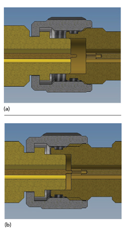
Figure 3 1.35 mm connector mating, showing engagement of the outer conductor centering cylinder (a) and engagement of the inner conductor pin (b).
In the world of mmWave connectors, the three cornerstones of design are tolerances, tolerances and tolerances. From the previous connector design discussion, dimensional integrity was enforced with various design choices, such as a centering sleeve on the pin side and a locking groove on the socket side. The connector is created from several machined parts whose dimensional integrity is limited by the sophistication and precision of the machining process. For a cable assembly there are additional factors, including cable construction, cable preparation (i.e., stripping three layers: the inner conductor, outer conductor and outer braid) and soldering the layers. The machined connector parts are metal (e.g., stainless steel and beryllium copper) and harder plastics (e.g., Ultem) that are manufactured to defined tolerances.
Applying tolerances to a cable that consists of multiple layers and materials that move in relation to one another, as well as applying heat to a solder joint, requires art as well as science. There are multiple, established cable designs; for this application, the combination of an extruded PTFE core for strength and robustness, a helical wrap outer conductor for superior electrical performance and stability and an outer braid for strength were chosen. Initial testing revealed electrical performance instabilities at E-Band that were not apparent at V-Band and below. Adding a layer between the outer conductor and the outer braid reinforced the rotational integrity of the helical wrap, providing extra dimensional support and eliminating the instabilities.
The solution to this problem underscores the known difficulty of the preparation and termination of a cable with a tape layer to the cable entry portion of the connector. This involves consideration of the tolerances for each of the strip lengths of the individual cable layers, i.e., the inner conductor, outer conductor and outer braid. In addition, each individual layer consists of a different base material, which necessitates a tailored stripping approach. While the intellectual understanding of soldering a two-stage ferrule is well understood, at mmWave wavelengths an iterative termination process was required - each time improving, learning and discovering. While the science of thoroughly documenting each step is important, equally important is the art of the skilled, experienced and intuitive technician.