
A dual-band continuous inverse class F mode power amplifier (PA) operates efficiently with a resistive third harmonic termination. Analysis predicts the effect of the resistive termination on drain efficiency and output power. Measurements demonstrate 10 W output power with 75 and 71 percent power-added efficiency (PAE) and greater than 13 dB gain at 0.8 and 2.4 GHz, respectively.
The rapid development of wireless communication technologies is driving the need for increased system bandwidth.1 The PA, a key transmitter component, is now expected to operate efficiently over broader frequency ranges. It is feasible to realize high efficiency and wideband performance with continuous modes;2 however, a multiband continuous mode PA is a better solution for high efficiency when frequencies extend beyond one octave. Harmonically tuned PAs, such as the continuous class F mode and continuous inverse class F mode, are used to achieve high efficiency. Unlike class A or B operation, harmonically tuned PAs require precise harmonic impedance control, as well as a proper fundamental impedance match. The continuous class F mode, for example, requires an infinite third harmonic termination, while the continuous inverse class F PA requires a short at the third harmonic.
Recent research in this area employed mixed class F and class F−1 modes to design a concurrent dual-band PA at 0.8 and 1.25 GHz.3 In another design, a dual-band harmonic control network was used to realize accurate harmonic terminations for high efficiency dual-band PA operation.4 Both obtained superior efficiency and output power at two operating frequencies; however, reactive third harmonic impedances are required, which inevitably results in a frequency conflict with a dual-band PA, when two operating frequencies f1 and f2 meet the condition 3f1 = f2. In this case, the third harmonic load for operating frequency f1 must be reactive while the fundamental component for the frequency f2 must simultaneously be resistive. To resolve this conflict, this article proposes using a resistive third harmonic continuous inverse
class F mode design for a dual-band PA.
TRADITIONAL CONTINUOUS INVERSE CLASS F MODE
The classic inverse class F mode PA requires the drain voltage waveform to be a half sinusoid and the drain current waveform to be a square wave at the transistor’s intrinsic plane. A Fourier series expansion shows a half-sinusoidal drain voltage waveform contains even harmonics of the fundamental, while a square current waveform contains odd harmonics. Therefore, to achieve 100 percent drain efficiency, the ideal inverse class F amplifier requires all odd harmonics to be shorted and even harmonics to be open circuited.
The normalized drain voltage and current waveforms for the inverse class F mode can be expressed as
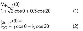
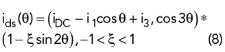
where iDC = 0.37, i1 = 0.43 and i3 = 0.06.
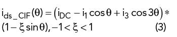
To realize the inverse class F mode precisely, short- or open-circuit transmission lines with high Q-factors are often used, typically limiting the bandwidth of the inverse class F mode to less than 10 percent. To address the bandwidth limitation, the performance of the continuous inverse class F mode amplifier is explored by attaching a factor, ξ, to the drain current waveform. The drain current waveform is then expressed as
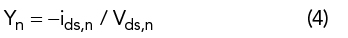
According to Equations 1 and 3, the fundamental and harmonic admittances in the continuous inverse class F mode can be expressed by the relationship
so that
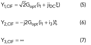
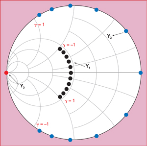
Figure 1 Design space of the continuous inverse class F mode.
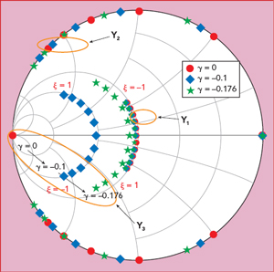
Figure 2 Fundamental and harmonic impedances vs. y.
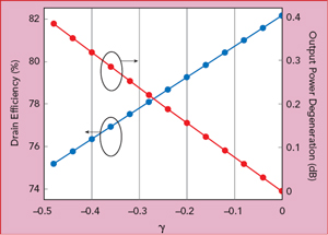
Figure 3 Drain efficiency and output power degeneration vs. y.
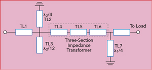
Figure 4 Topology of the output matching network.
Figure 1 shows the admittance distribution on the Smith chart. Compared with the traditional inverse class F mode amplifier, introduction of the parameter ξ extends the design space. By simultaneously varying the fundamental and second harmonic admittances on a circle of constant susceptance, this mode can deliver the same output power and drain efficiency as the standard inverse class F amplifier.5 Although the second harmonic admittance, Y2, is no longer restricted to an open circuit on the Smith chart, a short-circuited third harmonic termination is still maintained.
RESISTIVE THIRD HARMONIC CONTINUOUS INVERSE CLASS F MODE
In the above discussion, the multiplication factor 1 − ξ sinθ was introduced in the expression for the drain current of the standard inverse class F PA. Similarly, the drain current waveform for a resistive third harmonic continuous inverse class F mode PA is defined as
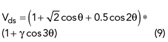
The voltage waveform is obtained by adding the multiplication factor 1 + γcos3θ to the voltage expression of the standard inverse class F mode amplifier:
Combining Equations 8 and 9, the fundamental, second and third harmonic admittances are derived:
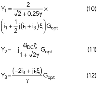
where Gopt represents the optimal admittance of the class B PA. A resistive third harmonic impedance is enabled with the introduction of the parameter γ. To prevent fundamental and third harmonic impedances from going beyond the Smith chart, γ must be restricted to be within −1 and 0.
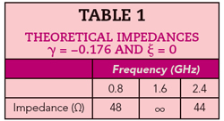
Figure 2 shows the theoretical fundamental, second and third harmonic admittances of the resistive third harmonic continuous inverse class F mode PA on the Smith chart. With γ decreasing, the third harmonic impedance gradually moves away from the short-circuit point; when γ decreases to −0.176, the third harmonic impedance approaches close to the fundamental impedance, and the fundamental impedance remains nearly constant.
Based on Equations 8 and 9, the drain efficiency (DE) and normalized output power (Pout) are calculated by
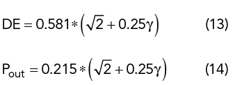
Output power degeneration is the difference between the output power of a traditional continuous inverse class F mode PA and the resistive third harmonic continuous inverse class F mode PA. Figure 3 shows the variation in DE and output power degeneration as γ varies from −0.5 to 0. With decreasing γ, DE decreases correspondingly, and efficiency greater than 78.5 percent is maintained with γ greater than −0.176. The output power remains nearly unchanged, as there is little variation of the fundamental impedance.
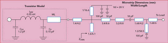
Figure 5 Output matching network with transistor parasitic model.
SIMULATION
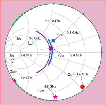
Figure 6 PA input and output impedances vs. frequency, with y = -0.176.
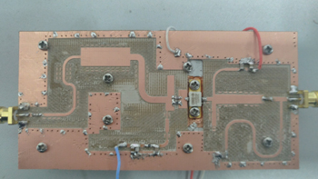
Figure 7 Assembled dual-band PA.
A dual-band PA operating at 0.8 and 2.4 GHz was designed to verify this analysis. To obtain the optimum impedances, an iterative load-pull simulation was employed from the low to high frequency. First, the optimal impedance was determined at 0.8 GHz by fundamental load-pull simulation with a proper harmonic impedance. Then, the optimal second harmonic impedance was obtained with harmonic load-pull simulation using the optimal fundamental impedance. In a similar manner, this process was repeated at 2.4, 4.8 and 7.2 GHz. Finally, γ was selected to be −0.176 with ξ = 0. Table 1 shows the theoretical impedances in this case.
Having determined the optimal impedances, the output matching network for the dual-band PA was designed. Figure 4 shows the design topology. For harmonic control at 1.6 GHz, a λ1/4 short-circuited transmission line, TL7, was used, where λ1 is the wavelength at 0.8 GHz. TL7 presents an infinite impedance at 0.8 and 2.4 GHz, so it does not affect the impedance match at either fundamental frequency. First, a λ2/4 short-circuit transmission line, TL2, and λ2/12 open-circuit transmission line, TL3, were used to present a short-circuit load at 4.8 and 7.2 GHz, respectively, where λ2 is the wavelength at 2.4 GHz. Then, TL1 with the proper characteristic impedance and electrical length was added to realize the harmonic impedances required. Finally, the fundamental impedance matches for 0.8 and 2.4 GHz were obtained with a three-section impedance transformer (TL4, TL5 and TL6), with the parameters calculated.
Figure 5 shows the final output matching network using a Wolfspeed CGH40010F transistor.6 The achieved impedance and targeted design space when γ equals −0.176 at the current generation plane are shown in Figure 6. These impedances are all located in the design space and close to the theoretical impedances in Table 1.
EXPERIMENTAL RESULTS
The Wolfspeed CGH40010F transistor was mounted on a 30 mil RF35 substrate with relative permittivity of 3.5 (see Figure 7). It was biased with −2.36 V at the gate and 28 V at the drain. A single tone continuous wave signal was applied, sweeping the input power from 18 to 30 dBm at each frequency (see Figure 8). With 28 dBm input power, the PA achieved a PAE of 75 percent at 41 dBm output power and 71 percent PAE with 41.4 dBm output power at 0.8 and 2.4 GHz, respectively. In both cases, the gain exceeded 13 dB. Figure 9 compares the simulated and measured PAE, gain and output power with 28 dBm input power over the two operating bands. Table 2 summarizes this performance, comparing it with similar published results.
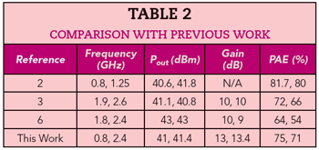
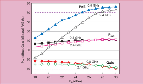
Figure 8 Measured Pout, PAE and gain vs. Pin at 0.8 and 2.4 GHz.
CONCLUSION
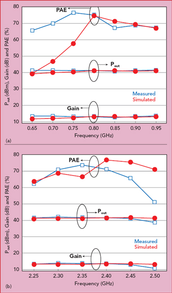
Figure 9 Measured vs. simulated Pout, PAE and gain vs. frequency in the lower (a) and upper (b) bands.
For a dual-band PA, a resistive third harmonic continuous inverse class F mode design provides a resistive third harmonic component to the complex fundamental impedance, solving the conflict when two operating frequencies f1 and f2 meet the condition 3f1 = f2. An efficient dual-band PA was simulated, built and measured, demonstrating the validity of this approach.
ACKNOWLEDGEMENTS
This work was supported by China Scholarship Council, the National Natural Science Foundation of China (61001012) and Teaching Research Project of Huazhong University of Science and Technology (15027).
References
- H. Huang, B. Zhang, C. Yu, J. Gao, Y. Wu and Y. Liu, “Design of Multi-Octave Bandwidth Power Amplifier Based on Resistive Second-Harmonic Impedance Continuous Class-F,” IEEE Microwave and Wireless Components Letters, Vol. 27, No. 9, September 2017, pp. 830-832.
- V. Carrubba, J. Lees, J. Benedikt, P. J. Tasker and S. C. Cripps, “A Novel Highly Efficient Broadband Continuous Class-F RFPA Delivering 74 Percent Average Efficiency for Octave Bandwidth,” IEEE MTT-S International Microwave Symposium Digest, June 2011, pp. 5-10.
- Y. Ding, X. Y. Guo and F. L. Liu, “High-Efficiency Concurrent Dual-Band Class-F and Inverse Class-F Power Amplifier,” Electronics Letters, Vol. 47, No. 15, July 2017, pp. 847-849.
- J. Pang, S. He, C. Huang, Z. Dai, C. Li and J. Peng, “A Novel Design of Concurrent Dual-Band High Efficiency Power Amplifiers with Harmonic Control Circuits,” IEEE Microwave and Wireless Components Letters, Vol. 26, No. 2, February 2016, pp. 137-139.
- V. Carrubba, A. L. Clarke, M. Akaml, Z. Yusoff, J. Lees, J. Benedikt, S. C. Cripps and P. J. Tasker, “Exploring the Design Space for Broadband PAs Using the Novel ‘Continuous Inverse Class-F Mode’,” IEEE European Microwave Conference, October 2011, pp. 10-13.
- P. Saad, P. Colantonio, L. Piazzon, F. Giannini, K. Andersson and C. Fager, “Design of a Concurrent Dual-Band 1.8 to 2.4 GHz GaN-HEMT Doherty Power Amplifier,” IEEE Transactions on Microwave Theory and Techniques, Vol. 60, No. 6, June 2012, pp. 1840-1849.