
Advanced semiconductor technology plays an important role in evolving RF and microwave applications for 5G and SATCOM where the next generation of systems is moving towards mmWave frequencies. Support of design flows and model availability for these semiconductor technologies is critical to designers for successful product development. In response, EDA software vendors offering MMIC and RFIC design solutions must work closely with leading foundries to ensure their products provide increased integration and higher performance while lowering cost and size requirements.
This article highlights techniques supporting device modeling of III-V wide bandgap semiconductor technology, specifically the United Monolithic Semiconductors (UMS) GH25 (0.25 µm gate length), GaN on SiC process for mmWave power amplifiers (PA) targeting new communication and defense systems. Model accuracy is validated through simulation and measurements of multiple designs that were developed using the GH25 process design kit (PDK), serving as a development framework that will guide future work in support of evolving process node technologies like the GH15, 0.15 µm GaN on SiC process currently in the qualification phase. Processes such as this are well suited for 5G applications as demonstrated by a 10 W Ka-Band (29.5 to 36 GHz) PA and a 2 W front-end module (24 to 30 GHz) that integrate the GaN on SiC PA with other RF functions implemented with a GaAs process.
GaN Technology and Modeling Challenges
Short gate-length GaN devices have demonstrated excellent performance for mmWave PAs. Offering higher operating voltages and reduced device parasitics, these GaN transistors provide higher output power densities, wider bandwidths and improved DC-to-RF efficiencies than their GaAs counterparts. In order to take advantage of this enhanced performance, designers need a scalable model that accurately captures the complex behaviors of the device during circuit simulation. The behavior of the trapping and thermal phenomena in GaN devices represents a real challenge for transistor modeling.
Devices can be represented in simulation by various methods, including compact, physics-based or behavioral models. Physics-based models incorporate physical aspects of the device to predict performance but are too complex for circuit simulation. Behavioral models are generally used in system simulations to represent an entire radio block but do not provide the necessary detail to support the actual amplifier design effort.
Compact models, based upon curve fitting, use functions and parameter values that produce the best fit to measured data, such as pulsed I/V and S-parameters. It is critical for the model to accurately replicate the transistor response over its entire range of operation in order to produce reliable circuit simulations. Parameters in these empirical models have no fundamental basis, but the physical consistency of the model equations is necessary to guarantee a good model extrapolation for designs lying outside the model characterization range.
There has to be a strong connection between technology/device development and the device modeling effort. The characterization and modeling methods implemented need to be validated through a well-established process/model qualification procedure that has been proven to yield reliable device models for the foundry’s family of semiconductor processes (see Figure 1). For GaN devices, the know-how and background from developing GaAs technologies have guided the current model development efforts in many cases. Established lower frequency GaN processes have also helped advance the state of device modeling for the latest short-gate devices. Nonlinear models are extracted taking into account traps phenomena1 and transistor self-heating. In addition to electrical characterization, the UMS modeling team performs a comprehensive study of the thermal device behavior and other non-stationary effects to improve the quality of their nonlinear device modeling.

Figure 1 Main steps to active device modeling incorporating measurements, model extraction and validation.
This fitting process and characterization data supports the development of transistor models used by software design tools, such as the NI AWR Design Environment platform, to predict the overall MMIC behavior when these devices are embedded in a matching/biasing network and excited by RF signals. Models are organized into PDKs supported in Microwave Office circuit design software with electrical and physical layout information to enable the design of MMICs using the GaN or GaAs process.
Model/PDK Development
Characterizing the active device to develop a scalable transistor model is the most important step in developing a process design kit. A scalable model allows the designer to vary the device periphery (gate width and number of gate fingers) for desired performance. One challenge is developing models accurately over the desired range of gate peripheries and operating conditions.
A device modeling procedure based on device characterization through measurement, model extraction via empirical fitting, and validation through device- and circuit-level simulation as illustrated in Figure 1 has been implemented here. The foundry also provides a family of models dedicated to multiple uses. For example, considering quarter micron technology, scalable linear models supporting low-noise amplifier (LNA) designs include noise characterization over a 10 to 20 V drain bias. A hot, nonlinear model for high power applications is scalable with medium to large gate peripheries, offering electrothermal model accuracy over a 10 to 30 V drain bias. A cold nonlinear model dedicated to switch applications is available for 2 topologies (serial and parallel) with model accuracy for various gate voltages.
Model Extraction
The typical equivalent circuit of a compact transistor model is shown in Figure 2. This model includes extrinsic linear elements and intrinsic nonlinear elements. Firstly, the transistor’s extrinsic parasitic elements (R, L and C) are extracted in order to de-embed the S-parameter data to the intrinsic reference plane and to extract the intrinsic parameters (Cgs, Cgd, Gm, Gd, Cds, Ri, Tau, Rgd) using explicit equations. The accurate extraction of the parasitic elements is based on both cold field-effect transistor (FET) S-parameter measurements (Vds = 0) and electromagnetic (EM) simulations of the device feed manifold.
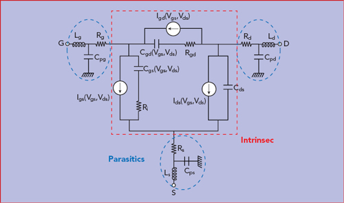
Figure 2 Nonlinear sources in equivalent circuit model with extrinsic parasitics.
The next step is to determine the value of the intrinsic elements. For GaN devices, the main nonlinearities are the drain-to-source current and the gate-to-source and gate-to-drain capacitor, as well as the input Schottky diode behavior.
The high-electron mobility-transistor (HEMT) is affected by trapping phenomena. Traps are locations within a semiconductor that limit the movement of holes, mostly due to crystalline imperfections in the GaN material like impurities in the crystal lattice and dangling bonds on the surface or at interfaces, as shown in Figure 3. These imperfections generate trap centers within the bandgap of a semiconductor.2 The parasitic charge of the traps affects the density of the two-dimensional electron gas channel3 in GaN-based transistors.
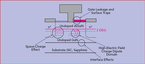
Figure 3 Locations of trapping centers in wide bandgap semiconductors.
A variety of trapping effects in aluminum GaN (AlGaN)/GaN HEMTs have been observed, including transconductance frequency dispersion, current collapse, gate- and drain-lag transients and restricted microwave power output. The dominant drain lag effect depends on both the voltage bias and the channel temperature, and it is traditionally taken into account by using quasi-isothermal pulsed I/V and pulsed S-parameter data instead of continuous wave (CW) measurements. The pulsed I/V S-parameters technique measures the S-parameters during the on-cycle of a fast pulse with a low-duty cycle. Instantaneous gate and drain biases are moved from a chosen steady quiescent bias to another point on the I/V plane to better replicate operational behavior where the thermal and trap conditions are set by the quiescent bias conditions (see Figure 4). Pulse widths are kept short enough to avoid a strong temperature variation during the pulse duration, so that the transistor’s pulsed I/V measurements are obtained under quasi-isothermal conditions.
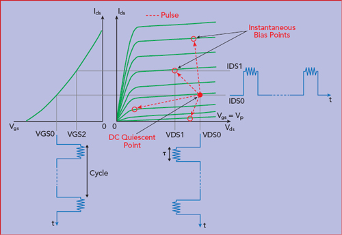
Figure 4 Pulsed technique for device characterization.
The data obtained with this measurement protocol is then used to fit the parameters of in-house equations, developed for improved accuracy of the source current derivatives (Gm/Gd) over large values of Vgs and Vds. Similarly, UMS gate charge equations improve the description of the capacitors variation over the gate and drain voltages.
Nevertheless, the pulsed I/V and S-parameter characterization are not sufficient for describing the drain lag in GaN transistors. Indeed, the trapping phenomena in GaN HEMTs present several time constants, some of them shorter than the shortest pulse duration available for test. The charge of these traps directly depends on the voltage pick across the device under RF dynamic operations, this is taken into account in the model by a dedicated module based on envelope detection.4
Thermal Modeling
The thermal behavior of high-power GaN devices must be taken into account. The thermal impedance is determined with the use of 3D finite-element method (FEM) simulation and introduced into the model using an electrical description in order to automatically calculate the junction temperature during the electrical simulation, as described in reference 4 (see Figure 5). The model is valid over a backside temperature from −40°C to 120°C. This electro-thermal model enables design at different temperatures and simulation of the junction temperature in both CW and pulsed operations.
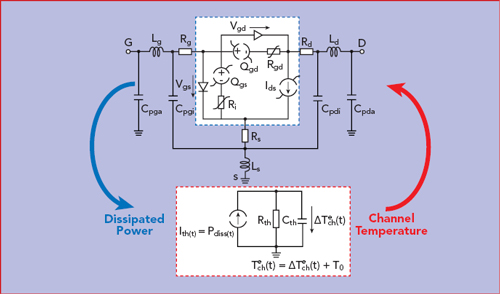
Figure 5 Electrical description of the thermal behavior of the device contained in the model.
Model Validation
The resulting model is validated by comparing simulation results for a range of operating conditions and gate peripheries (from 2 x 30 µm to 10 x 300 µm for this quarter micron process). Load-pull measurements are used to validate the model’s ability to predict device performance for different load impedances. For validation, the model is used for a fixed device periphery at various bias conditions, input power levels and excitation frequencies. Load-pull simulations in Microwave Office software can be readily compared to measured results obtained in the test lab. Measured figures of merit, such as gain, output power, power-added efficiency (PAE) and drain current, are captured in Figure 6 for a 1 mm device operating at 10 GHz, and show excellent agreement with the simulation results at several backside temperatures sweeping from −40°C to 125°C. The load positions for optimum power, PAE or linearity are also well-simulated as demonstrated in Figure 6 by the output power contour load pull.