
TECHNICAL FEATURE
Adaptive Feedforward Amplifier Linearizer Using Analog Circuitry
Alfonso J. Zozaya,
Eduard Bertran Albertí
and Jordi Berenguer-Sau
Dept. of Signal Theory and Communications
Polytechnic University of Catalonia
Barcelona, Spain
Nowadays, feedforward is the most effective and broadly used linearization technique employed in modern multi-carrier communications systems. Different versions, in which the key operating parameters are adjusted by means of some mechanisms of automatic adaptation, have been developed and patented.15 The key aspects of the feedforward linearization technique are the amplitude and phase imbalances as well as the inequality of the signal delays among the different branches which are compared. In this article a brief description of a typical feedforward architecture is made and the simulation results of a compensation technique for these imbalances using the least mean square (LMS) algorithm, implemented entirely in the analog domain, are presented.
FEEDFORWARD TECHNIQUE
The architecture of the well-known feedforward linearizer has the form illustrated in Figure 1. Since the power amplifier (PA) presents amplitude and phase distortion, it will be assumed that its out-put is made up of an amplified version of the input signal plus certain intermodulation (IMD) products. These IMD products occupy the same frequency band as the input, the in-band distortion and a spectrum of frequencies outside of the band of interest, the out-of-band distortion. Ideally, the linearization technique of the amplifier aims to eliminate completely the distortions present in the PA output signal. Following this argument the principle of operation of the feedforward linearizer will be described.
|
|
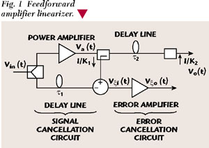
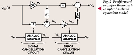
The feedforward linearizer consists of two fundamental circuits -- the signal cancellation circuit and the error cancellation circuit. In the former, an error signal that contains the IMD products generated in the PA is obtained. This error signal is the result of the comparison of a sample of the PA output signal, appropriately attenuated, with a properly retarded sample of the input signal. This combination is usually carried out in a 180° combiner.1 In the latter, the error cancellation circuit, the error signal obtained in the previous circuit is appropriately amplified and injected in opposite-phase to the output to cancel the IMD introduced by the PA. Before the combination, the PA output is suitably delayed. The combination of the error signal with the PA output signal usually takes place in a power directional coupler.1 For simulation purposes the equivalent complex baseband model is shown in Figure 2. The delays among the branches are theoretically compensated. The PA and the error amplifier are represented by the complex gains G and g, respectively. While G is a function of the input signal amplitude, g is assumed to be a constant, which implies a linear operation of the error amplifier. The terms 1/k1 and 1/k2 represent the coupling factors of the directional couplers used in the signal cancellation circuit and the error cancellation circuit, respectively. The complex quantities a and b constitute adjustable parameters for the compensation of the gain and phase imbalances among the branches that are compared.
|
|
The PA input, in a generic case, can contain several independent digital signals, and each one can carry information as much from the phase as in the amplitude. In the first approach, a single input signal is assumed that only carries information with regard to phase, with a complex envelope of the form
vin = cej (t) (1)
As previously mentioned, the nonlinear PA introduces amplitude and phase distortion. Taking as reference the signal from Equation 1, the PA output is
Va = Gl vin + vIMD (2)
where
Gl = |Gl |ej = the linear gain of the PA
Gl vin = amplified version of the input signal plus a certain phase shift
vIMD = intermodulation products
In the signal cancellation circuit a fraction of the PA output signal va /kl , with kl real, is compared with a sample of the input signal avin , with a complex, resulting in an error signal v*i given by
If a is adjusted in such a way that
the error signal **i will contain only the intermodulation products.

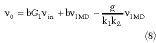
In order to adjust these gain and phase imbalances accurately, the complex parameter a will be altered by means of an adaptive procedure. In a similar way, in the error canceling circuit, the error signal is amplified in a second amplifier, the error amplifier, to obtain
v 0 = gv i (6)
g = |g| ejß is the gain of the second amplifier. In a way similar to the previous case, the gain and phase of the signal va will be adjusted by means of the complex parameter b, before comparing it to the signal v 0 to obtain an output signal v0 free of distortions
where k2 is real.
If b is adjusted such that

the equation for *0 becomes
v0 = bGvin (10)
The complex parameter b will be adjusted by means of an adaptive algorithm similar to the one used with the parameter a.
Currently, an exact evaluation of the parameters a and b in order to achieve an exact error signal as in Equation 5 and an output signal free of intermodulation products as in Equation 10, respectively, presents insurmountable theoretical and practical difficulties. From a theoretical point of view, if the time delays among the different branches are assumed to be equal, a cancellation of the intermodulation products is possible for the simple case presented previously. The situation becomes more complicated if the input signal presents a time-varying amplitude. In this case the PA complex gain will also vary with time as a function of the amplitude of the input signal. Consequently, it will be impossible to cancel the input signal completely in the signal canceling circuit, unless the parameter a could be adjusted with a higher speed than the speed of change of G. If, on the other hand, the case of an input signal made up of several digital signals such as the one described in Equation 1, with each having a different carrier, is considered, it will be impossible to obtain their total cancellation in the signal canceling circuit by using only one correction loop. In principle, to obtain the intermodulation products, it will be necessary to include as many correction loops as there are different carriers.
Practically, the accuracy in the estimate of the parameters a and b is limited by the amount of processing that is used and by the inherent limitations of the adaptive methods employed. A detailed analysis of the different methods used for the estimate of the parameters a and b is outside the purpose of this article and is a topic open to new possibilities.
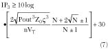
The equality shown in Equation 9 can be achieved only for values of g/k1 k2 ≈ 1 and therefore the error amplifier gain must be comparable to the coupler losses 1/k1 k2 . In these circumstances, the linearity premise of the error amplifier supposes an operating point much below saturation. If its 1 dB compression point is comparable with that of the main amplifier, such an operation is allowed because the input signal of the error amplifier is composed only of the IMD terms. Some practical considerations on this problem are presented by Cripps.1 There is a compromise between the amount of IMD reduction and the error amplifier compression characteristics.
ADAPTIVE SOLUTION
An effective and recent solution for an adaptive estimate of the complex parameters a and b includes the use of digital signal processing (DSP) in both cancellation circuits. In this approach, the convergence of the signal canceling circuit must be achieved first in order to avoid stability problems.2
A similar adaptive structure in which the processing is carried out entirely in the analog domain is proposed instead of using a digital architecture based on DSP. This solution supposes great robustness and circuit simplicity, but in its basic version does not allow a precise estimate of the parameters a and b. The analyses will start first with a basic architecture and then the hardware will be expanded to increase the precision of the estimate of the parameters a and b gradually, until an acceptable level is achieved.
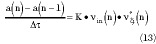
The complex parameters a and b will be adjusted according to the LMS algorithm implemented in the analog domain. Only the equations corresponding to the adaptation of parameter a are developed with the assumption that the same ones are completely applicable to the parameter b.
According to the LMS algorithm, the equations for a are given by
a(n) = a(n 1) + Δ  vin (n)
  (n) (11)
a(n) a(n 1) =
K Δ  vin (n) (n) (12)
where
K = constant of adaptation that fixes the algorithm adaptation speed
vin ( ) = PA input signal
( ) = complex conjugate of the error signal described by Equation 3
Equation 12 can take the equivalent form
Taking the limit for * approaching zero and assuming a(*) to be analytic,

and the actual expression for a is obtained as
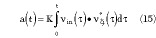
Equation 15 can be implemented in baseband, or in a relatively low intermediate frequency (in an analog way) using operational amplifiers and analog four-quadrant multipliers.
The functional block illustrated in Figure 3 represents a four-quadrant multiplier (FQM).
|
|
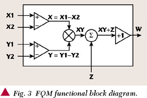
Taking into account that
vin ( ) = vinI + jvinQ ( I + jv  iQ ) (16)
where the sub-indexes I and Q refer, respectively, to the in-phase and quadrature components of the corresponding signal. It follows that
vin v* i = (vinI v iI
+ vinQ v* iQ )
+ j(vinQ v* I vinI
v iQ ) (17)
Considering the previous result, eight four-quadrant multipliers will be required -- four for the multiplication
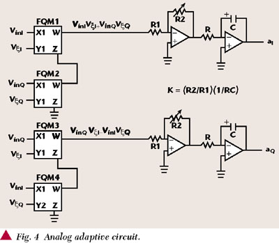
vin ( ) v* i ( ) for the estimate of parameter a, and four for obtaining the product v i ( ) * v* o ( ) to estimate parameter b. The sums required in each complex multiplication as well as the conjugation of the factors could be implemented using the same FQM. The resulting analog adaptive circuit is shown in Figure 4.
|
|
SIMULATION RESULTS
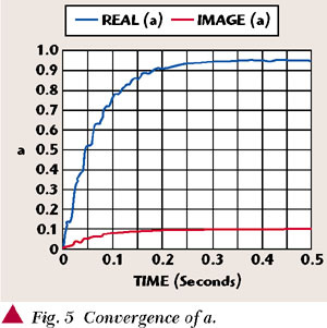
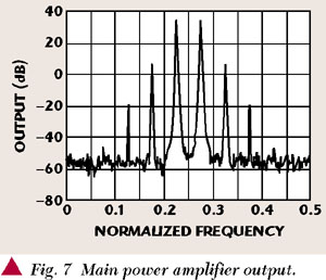
The architecture shown in the complex baseband equivalent circuit has been simulated for an input signal made up of two tones at 0.1 and 0.15 Hz per sample, respectively. Figure 5 shows the convergence curves for parameter a, while Figure 6 shows the convergence curves for parameter b. In Figures 7, 8 and 9 the spectra of the signals of interest are illustrated starting from which the proposed solution can be arrived at.
|
|
|
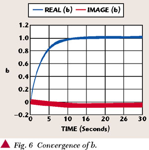
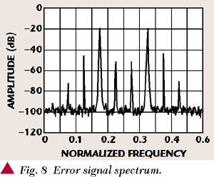
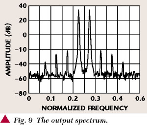
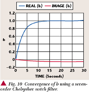
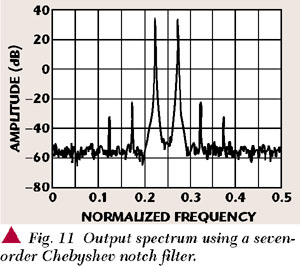
It can be seen from the convergence of b that it exhibits a high misadjustment. The superimposed noise on parameter b has the same form as the input signal vin ( ) and is due to the higher power of this signal compared with the IMD products that it is expected to suppress. This situation does not allow a reduction of all the IMD harmonics and, on the contrary, the smaller power IMD components are magnified. The described situation can be appreciated when comparing the output spectrum with the main power amplifier output. This unwanted effect can be eliminated by using a notch filter that suppresses the signal in the LMS adapter that estimates a, as proposed by S.J. Grant.2 Using a Chebyshev seven-order notch filter with a stop-band that coincides with the vin bandwidth, an acceptable result is achieved. The curve of convergence of the parameter b is notably improved (Figure 10) and the harmonic of smaller power are discriminated and suppressed at the output (Figure 11).
|
|
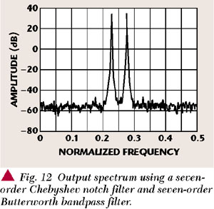
The IMD reduction achieved is appreciably better but it is not of the typical order of magnitude reported in the references1,2,4,5 for the same linearization technique. The apparently hidden reason resides on the way the parameter a is obtained. Indeed, in the error signal spectrum shown, the wanted signal is considerably reduced, but at the price of introducing additional intermodulation components in quadrature with the intermodulation components that are expected to be eliminated. The problem is solved again by limiting in frequency the correlation of the signals vin and v i to the band of the signal vin with a seven-order bandpass Butterworth filter. The spectrum of the output signal is illustrated in Figure 12 for this case.
|
|
CONCLUSION
An acceptable estimate of the complex parameters a and b for the amplitude and phase imbalances compensation in the signal cancellation circuit and the error cancellation circuit, respectively, of a feedforward linearizer was possible, using analog processing of the corresponding signals. A basic adaptive structure based on the analog LMS algorithm was analyzed and simulated. With the basic architecture, a 30 dB reduction of the larger harmonics was attained, but those of smaller power were lightly magnified. By including two seven-order Chebyshev notch filters in the estimate of b this unwanted effect was eliminated. By including two seven-order Butterworth bandpass filters in the estimate of a, an IMD reduction of 50 dB was achieved. Although the latter result is similar to those accomplished by means of other implementations of the feedforward linearization technique, the current realization exhibits the added advantage that the circuitry is totally analog, and can be implemented with simple hardware. *
References
1. S.C. Cripps, "RF Power Amplifiers for Wireless Communication," Artech House, 1999, pp. 267279.
2. S.J. Grant, J.K. Cavers and P.A. Goud, "A DSP Controlled Adaptive Feedforward Amplifier Linearizer," Proc. IEEE Intl. Conf. Universal Personal Commun, Cambridge, MA, Sept. 29Oct. 2, 1996,
pp. 788792.
3. J.K. Cavers, "Adaptive Feedforward Linearizer for RF Power Amplifiers," US Patent Serial No. 5,489,875, February 6, 1996.
4. Q. Cheng, C. Yiyuan and Z. Xiaowei. "A 1.9 GHz Adaptive Feedforward Power Amplifier," Microwave Journal, Vol. 41, No. 11, November 1998, pp. 8696.
5. W.T. Thornton and L.E. Larson. "An Improved 5.7 GHz ISM-band Feedforward Amplifier Utilizing Vector Modulator for Phase and Attenuation Control," Microwave Journal, Vol. 42, No. 12, December 1999, pp. 97106.
|
Alfonso J. Zozaya earned his degree in electronic engineering from the Polytechnic University of the National Armed Forces, Maracay, Venezuela, in 1991. In 1994 he became an assistant professor in the electronic and communication department of the University of Carabobo, Valencia, Venezuela. He is currently working on his PhD in the area of RF power amplifier linearization using the hyperstability theory in the department of signal theory and communications of the Polytechnic University of Catalonia, Barcelona, Spain. Eduard Bertran Albertí received his telecommunication engineering degree and doctorate in telecommunications in 1979 and 1985, respectively, from the Polytechnic University of Catalonia (UPC). He became a lecturer at UPC in 1980, and joined the department of signal theory and communications in 1987, where he is currently an associate professor. He has been the head of studies of the department and an associate dean in different telecommunications schools. His research is focused in control, signal processing and circuit theory, and he has collaborated in different national and European research projects. He is the author of 24 articles and book chapters, and about 30 conference papers. He holds a patent on amplifier linearization. Jordi Berenguer-Sau received his telecommunication engineering degree and doctorate in telecommunications in 1984 and 1988, respectively, from the Polytechnic University of Catalonia (UPC). In 1988 he joined Mier Comunicaciones as head of the RF laboratory. In 1992 he joined the department of signal theory and communications at UPC as an associate professor. His main research activities are the design of microwave and RF systems and applications. |