
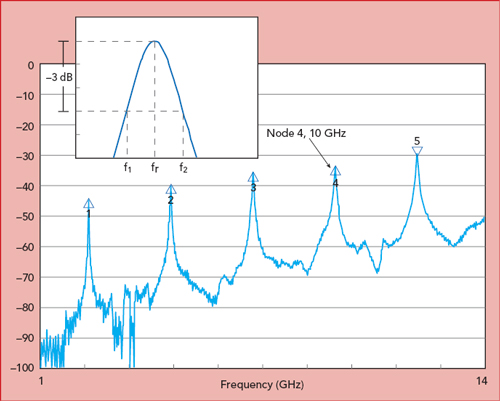
Figure 2 Wideband clamped stripline measurement of a MUT 60 mils thick, with a Dk = 3.48.
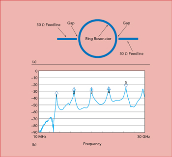
Figure 3 Microstrip ring resonator (a) and wideband measurement (b).
Figure 2 shows a measurement using the clamped stripline test method with a 60-mil thick MUT with Dk = 3.48.
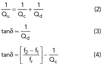
Ring resonators are often used as test circuits.3 They are simple microstrip structures having resonances at integer multiples of the mean circumference of the microstrip ring (see Figure 3a). They are typically loosely coupled, as loose coupling between the feed lines and the ring minimizes the capacitance of the gaps between the feed lines and the ring. This capacitance changes with frequency, causing the resonant frequency to shift and resulting in errors when extracting the material Dk. The conductor width of the resonator ring should be much smaller than the radius of the ring - as a rule of thumb, one-quarter the dimension of the ring radius or smaller.
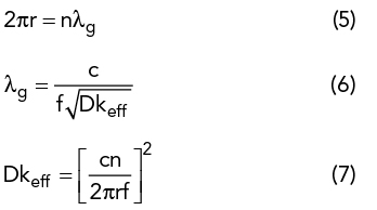
The |S21| response of a microstrip ring resonator on a 10-mil thick circuit material with Dk = 3.48 is shown in Figure 3b. An approximate calculation of the Dk is given by
Although approximate, these formulas are useful for determining an initial Dk value. A more accurate Dk can be found using an electromagnetic (EM) field solver and precise resonator circuit dimensions.
Loosely coupled resonators are often used for Dk and Df measurements to minimize resonator loading effects. Coupling should be loose enough so the insertion loss is 20 dB or less at the resonant peak. In some cases, with extremely weak coupling, the resonant peak may be so weak that it cannot be measured. This typically occurs for resonant circuits with thinner substrates, the types of materials commonly used in mmWave applications, since the high frequencies have small wavelengths and circuit dimensions.
mmWAVE TEST METHODS
While there are many Dk test methods, only some are suitable for mmWave frequencies, yet none are accepted as industry standards. However, the following methods are accurate and repeatable at mmWave.
Differential Phase Length Method
The microstrip differential phase length method has been used for many years.4 It is a transmission test method in which phase measurements are made on two circuits that only differ by physical length (see Figure 4). To avoid any variations in circuit material properties, the circuits are fabricated side-by-side and as close together as possible on the MUT. The circuits are 50 Ω microstrip transmission lines of different lengths with a grounded coplanar waveguide (GCPW) signal launch. At mmWave frequencies, the GCPW signal launch is important, since the launch area can have a major impact on return loss. End-launch connectors should also be used, to make good pressure contacts between the coaxial connectors and the test circuit without soldering, allowing the same two connectors to be used for the shorter and longer circuits. This minimizes the effect of the connectors on measurement results. For consistency, the same connectors should be oriented to the same ports of the vector network analyzer (VNA). If connector A is oriented to port 1 of the VNA and connector B to port 2 for testing the shorter circuit, the same should be true when testing the longer circuit.
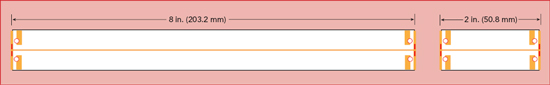
Figure 4 Top view of the long and short microstrip circuits used in the differential phase-length method.
Subtracting the phase angles of the short and long circuits will also subtract the effects of the connectors and the signal launch areas. If the return loss is good for both circuits and the connectors have consistent orientation, most of the effects of the connectors will be minimized. When using this method at mmWave frequencies, return loss at these transitions of better than 15 dB through 60 GHz and 12 dB from 60 to 110 GHz is considered acceptable.
The extraction equations for the microstrip differential phase length method are based on a manipulation of the microstrip phase response formula for circuits with different physical lengths:
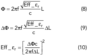
where c is the speed of light in free space, f is the frequency of the S21 phase angle, ΔL is the difference in physical lengths of the two circuits and ΔΦ is the difference in phase angle between the shorter and longer circuits.
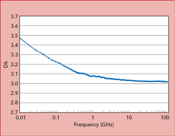
Figure 5 Dk vs. frequency measured with the microstrip differential phase length method.
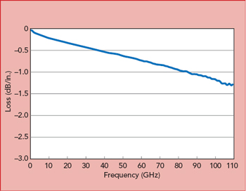
Figure 6 Insertion loss vs. frequency determined from the microstrip differential length measurements.
The test method comprises a few simple steps:
- Measure the S21 phase angle as a function of frequency for the shorter and longer circuits.
- Use the formulas to determine the measured effective Dk.
- Obtain precise and accurate circuit dimensions that can be entered into an EM field solver using the initial Dk value for the material.
- Use the software to generate a simulated effective Dk value. Change the Dk in the solver until the measured and simulated effective Dk values for the material match at the same frequency.
- By incrementing the frequency into the mmWave region and repeating this process, the Dk value can be determined across a range of frequencies through mmWave.
Figure 5 shows a measurement using the microstrip differential phase length method with 5-mil thick RO3003G2TM circuit material. The curve was generated using a Microsoft Windows PC program developed by Rogers Corp.5 The data reflects the usual trend of decreasing Dk with increasing frequency. At lower frequencies, larger changes in Dk occur versus frequency; however, from 10 to 110 GHz, the Dk shows little change. This curve reflects a material with low loss and rolled copper with a smooth surface. A material with high loss and/or higher copper surface roughness will exhibit an increased negative slope in the Dk-frequency relationship. Using this test method, the insertion loss for circuits using the MUT can be obtained by subtracting the S21 values of the shorter and longer circuits at each frequency (see Figure 6).
Ring Resonator Method
The ring resonator method is another approach for mmWave characterization. While ring resonators are often used below 10 GHz, with proper fabrication precision they can be used effectively at mmWave frequencies. Fabrication is important because the effects of circuit dimensions and dimensional tolerances are greater at mmWave, with any variation reducing accuracy. The thickness of the copper plating on the circuit material also varies, as does the gap dimension. Most mmWave ring resonators are thin (usually 5 mils), and the gap between the feed line and resonator ring is also small. Thickness and gap variations for a gap-coupled ring resonator will impact both coupling and the resonant frequency.
When comparing two circuits built on the same circuit material and with different copper plating thicknesses, the circuit with the thicker copper will exhibit a lower Dk. The resonant frequencies of the two circuits will also differ, even though they should be the same for the same circuit material and test method. Figure 7 shows an example where the thickness variation in a circuit’s final plated finish causes differences in the extracted Dk for the same material. Whether the finish is electroless nickel immersion gold (ENIG) or other plated finishes, the issue remains.
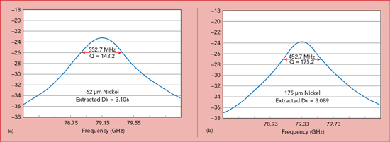
Figure 7 mmWave ring resonator measurements of a MUT with 62 μm thick (a) and 175 μm thick (b) nickel plating.
Besides these fabrication issues, conductor width variation, etched-space variation, trapezoidal effects and substrate thickness variation cause similar effects. If all these variations are accounted for, one individual ring resonator measurement can yield the correct Dk value; however, many test routines will assume nominal circuit dimensions and extract an incorrect Dk. At lower frequencies these effects do not impact Dk accuracy as much as at mmWave frequencies.
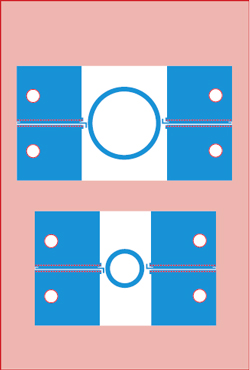
Figure 8 Test rings used with the microstrip differential circumference ring resonator method.
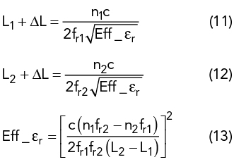
Another significant variable using ring resonators at mmWave is the gap coupling changing with frequency. It is typical for ring resonators to be evaluated using multiple nodes, with the nodes usually spaced by significant differences in frequency. As a result, gap coupling variation can be a significant source of error. To overcome this, a differential circumference method is used. This approach uses two ring resonators, essentially identical except the ring circumferences differ in size and are integer multiples of each other (see Figure 8). With two ring resonators, the higher order resonant nodes used in the Dk extraction have some frequencies in common. Since the feed lines and gaps are the same, the effects of gap coupling are decreased - theoretically eliminated - which leads to better accuracy in the extracted Dk. The Dk is calculated from the equations:
The ring resonators in Figure 8 are microstrip structures, with the feed lines tightly-coupled GCPW to avoid open-end feed line resonances, which could interfere with the ring resonant peaks. If the feed lines were open-ended microstrip, they would have their own resonances. The only way to avoid this is to make the feed lines much shorter or use tightly-coupled GCPW feed lines. Since the differential circumference ring resonator method yields the circuit’s effective Dk, it is still necessary to make accurate circuit dimension measurements and use a field solver to extract the material Dk.
CONCLUSION
The mmWave test methods discussed here are circuit-based. Several other methods may be considered, such as raw material tests, but most yield a material Dk for the x-y plane rather than the z-axis (thickness). Circuit designers are more interested in the z-axis Dk, but for those willing to work with x-y material Dk values, free-space measurements, split-cylinder resonator measurements and waveguide perturbation testing are additional test methods.
The clamped broadside coupled stripline resonator test method has also been evaluated for determining circuit material Dk at mmWave frequencies. Unfortunately, this approach is most effective with small pieces of MUT and is not practical for volume testing. The quest continues to find a good raw material test to characterize materials at mmWave frequencies.
References
- L. F. Chen, C. K. Ong and C. P. Neo, “Microwave Electronics, Measurement and Material Characterization,” John Wiley & Sons Ltd., 2004.
- IPC-TM-650 Test Method Manual, “Stripline Test for Permittivity and Loss Tangent (Dielectric Constant and Dissipation Factor) at X-Band,” IPC, March 1998, pp. 1–25.
- K. Chang and L. H. Hsieh, “Microwave Ring Circuits and Related Structures,” Wiley-Interscience, division of John Wiley & Sons, New York, 2004.
- N. K. Das, S. M. Voda and D. M. Pozar, “Two Methods for the Measurement of Substrate Dielectric Constant,” IEEE Transactions on Microwave Theory and Techniques, Vol. 35, No. 7, July 1987, pp. 636–642.
- “ROG Dk Calculator,” Rogers Corp. Technology Support Hub. www.rogerscorp.com/acs/technology/index.aspx.