
The dielectric constant (Dk) or relative permittivity of a circuit material is not a constant - despite what its name might imply. The Dk of a printed circuit board (PCB) material, for example, will change as a function of frequency. Also, using different Dk test methods on the same piece of material, they are likely to measure different Dk values, which are correct for those test methods. As circuit materials are increasingly employed at mmWave frequencies, with the growth of 5G and advanced driver assistance systems, it is important to understand how Dk changes with frequency and which Dk test methods are “best” applied.
No industry-standard best test method exists for measuring circuit material Dk at mmWave frequencies, although organizations such as the IEEE and IPC have committees devoted to this topic. It is not the lack of measurement methods; in fact, more than 80 are described in just one reference by Chen et al.1 No method is ideal, with each having challenges and shortcomings, especially at frequencies from 30 to 300 GHz.
CIRCUIT vs. RAW MATERIAL TESTS
Tests for determining circuit material Dk or Df (the loss tangent or tanδ) are generally performed in one of two ways: either on the raw material or a circuit fabricated from the material. Raw material tests depend on high quality test fixtures and test equipment to extract Dk and Df values directly from the material. Circuit tests use a common circuit and extract the material parameters from the circuit’s performance, such as measuring the center frequency or frequency response of a resonator. Raw material tests introduce uncertainties typically associated with the text fixture or test setup, while circuit tests contain uncertainties from the test circuit design and fabrication techniques. Because the two methods differ, measurement results and accuracy levels typically do not agree.
For example, an X-Band clamped stripline test defined by IPC,2 a raw material test, may not provide Dk results agreeing with a circuit test of the same material. The raw material test creates a stripline resonator by clamping two pieces of the material under test (MUT) in a special test fixture. Air can become entrapped between the MUT and the thin resonator circuit which is part of the fixture. The air becomes part of the measurement and lowers the measured Dk. If a circuit test is performed on the same circuit material, without the entrapped air, the measured Dk will be different. For a high frequency circuit material with a Dk tolerance of ±0.050 determined from a raw material test, a tolerance of ±0.075 may result from a circuit test.
Circuit materials are anisotropic, often with different Dk values in the three material axes. Dk values typically differ little between the x- and y-axis, so for most high frequency materials, Dk anisotropy comparisons are usually made between the z-axis and the x-y plane. For the same MUT, test methods that measure Dk for the z-axis can provide different results than test methods used to evaluate Dk in the x-y plane, although the values of Dk may be “correct” for the given method.
The type of circuit used for a circuit test also influences the value of the measured Dk. In general, two types of test circuits are used: resonant structures and transmission/reflection structures. Resonant structures typically provide narrowband results, while transmission/reflection tests are usually wideband. Methods using resonant structures are typically more accurate.
TEST METHOD EXAMPLES
An example of a raw material test is the X-Band clamped stripline method. It has been used by manufacturers of high frequency circuit laminates for years and is a dependable means of determining the Dk and Df (tanδ) in the z-axis of a circuit material. It uses a clamping fixture to form a loosely coupled stripline resonator from MUT samples. The measured quality factor (Q) of the resonator is the unloaded Q, so it can be measured with minimal impact from cables, connectors and fixture calibration. The MUT is a copper-clad circuit laminate with all the copper etched from the substrate prior to testing. The raw circuit material is environmentally conditioned, cut to size and placed into the fixture on both sides of the resonator circuit at the signal plane (see Figure 1).
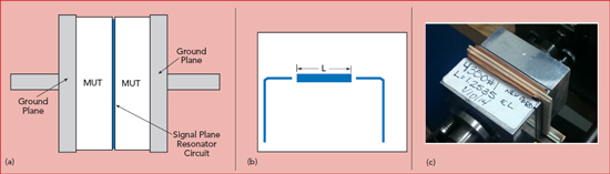
Figure 1 X-Band clamped stripline test fixture side view (a), stripline resonator (b) and photograph (c).
The resonators are designed with half-wavelength resonances starting at about 2.5 GHz, so node 4 is around 10 GHz; this is the node commonly used for Dk and Df measurements. Lower nodes and frequencies can be used - even the higher node 5 can be used, although higher nodes are usually avoided due to wave propagation or measurement issues from harmonics and spurious content. The extraction of the Dk or relative permittivity (εr) is straightforward:
where n is the node, c is the speed of light in free space and fr is the center frequency of the resonant peak. ΔL compensates for the electrical length extension due to electric fields in the gap-coupled area. Extraction of tanδ (Df) from the measurements is also straightforward. It is a fraction related to the 3 dB bandwidth of the resonant peak after subtracting the conductor losses (1/Qc) associated with the resonator circuit.