
Material Model Identification
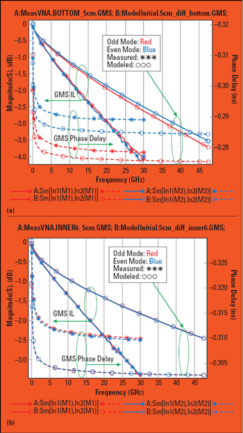
Figure 7 Measured (stars) and modelled without roughness (circles) GMS insertion loss and phase delay for 5 cm differential segment in layers BOTTOM (a plot, microstrips) and INNER6 (b plot, striplines).
For material parameters identification, we used measurements obtained with 50 GHz VNA and electronic calibration kit. The measurements with the mechanical calibration kit are used to identify the copper resistivity for INNER6 layer only (used for all conductors).
Generalized modal insertion loss and phase delay for differential microstrip and striplines are shown in Figure 7 as an example of the initial measurement to simulation comparison. We can observe some differences in the modal phase delays - the model with manufacturer data predicts lower delays. More importantly, the measured and simulated modal insertion losses are dramatically different. Such difference makes any analysis with the spreadsheet or manufacturer data completely useless above about 3 GHz. This is due to the absence of data for the roughness model.
There are multiple ways to proceed with the material models identification4,5. Typically, raw or de-embedded S-parameters are used to “tune” a corresponding model (sometimes called “model calibration”). This is an acceptable technique, but it is too complicated due to the large number of non-zero S-parameters in the case of differential traces. The simplest way is to use just two GMS-parameters and the following formal process (identification with dielectric and conductor loss separation):
1. Identify copper resistivity by matching measured and simulated GMS insertion loss (GMS IL) at the lowest frequencies.
2. Identify dielectric constant (Dk) by matching measured and simulated GMS phase delay (GMS PD).
3. Identify loss tangent by matching GMS IL at lower frequencies (below 1 to 2 GHz) and re-adjust Dk to match GMS PD (changes in LT can affect the delay).
4. Identify the roughness model parameters by matching GMS IL at high frequencies (above 2 to 3 GHz) and re-adjust Dk to match GMS PD (roughness can also affect the delay).
5. Do it for all unique dielectrics in the stackup.
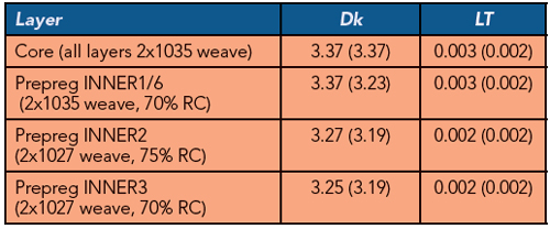
There are multiple ways to proceed with the material identification for this stackup. One option is to stick with the core/prepreg stackup structure and identify one model for the core dielectric and three models for the stripline prepreg layers. The table lists identified Wideband Debye models with Dk and LT at 1 GHz (the PCB manufacturer’s spreadsheet data are in the brackets for comparison):
Causal Huray-Bracken models8 with parameters SR = 0.098 μm, RF = 12.5 are used for all stripline layers. A non-causal model would produce about 2 ohm difference between the measured and modelled TDR impedance.8 Conductor resistivity was adjusted to 1.2 of the resistivity of the annealed copper. Note that the “prepreg” and “core dielectric” parameters came relatively close to the spreadsheet data. This model would be perfect, except for one limitation. There will be too small a difference in the propagation velocity for the odd and even modes in the differential striplines to account for the far-end cross-talk observed in the measurements.
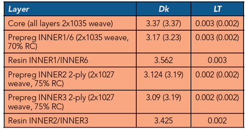
To account for the inhomogeneity of the layered dielectric, additional resin-rich layers around the strips are defined. “Resin-rich” in this context does not mean that this is a resin layer. It may contain different components that make properties of this composite material different from the layer with the fabric. The table on page 29 lists identified Wideband Debye models with Dk and LT at 1 GHz (PCB manufacturer spreadsheet values are in the brackets).
The conductor and conductor roughness models are the same as for the previous case. The material parameters for the microstrip layer were the same for the two cases with Dk = 3.40 (3.19), LT= 0.006 (0.002) for prepreg and Dk= 3.2 (4.0), LT= 0.02 for the solder mask (both Wideband Debye models at 1 GHz). Causal Huray-Bracken model parameters for the microstrip layer are SR= 0.229 μm, RF = 3.77 (rougher copper is used for the surface layers). Correspondence of the measured and identified GMS-parameters is shown in Figure 8. There is a small difference in the phase delays of the even and odd modes in the strip layers (sufficient to account for the observed far-end cross-talk at about −30 dB). Everything finally looks good, and we are ready to proceed with the validation step.
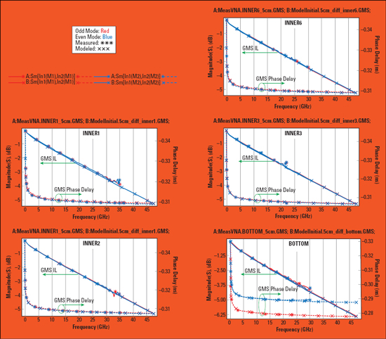
Figure 8 Measured (stars) and simulated (x-s) GMS insertion loss (IL) and phase delay (PD) for diff. transmission lines in all unique layers.
Validation
At the validation step, we simulated all structures on the board using the trace width and shape adjustments as well as the dielectric and conductor roughness models identified earlier. The layered dielectric structure with the “resin-rich” layer was used for all transmission line segments. No further adjustments were performed. The goal here is not getting a good fit between the measurements and models by tuning the model parameters and showing that we can achieve excellent correlation, but rather to see what accuracy can be achieved based on the formal material identification and limited number of cross-sections. This is the most important step to have confidence in the manufacturing, measurements, and modelling to reveal the potential problems.
To start the validation, we had to decide what was going to be modelled. We could either de-embed the connectors and launches from the measured data (simpler models) or create models of the measured links with the coaxial connectors and launches. De-embedding on PCBs is notoriously difficult due to the manufacturing variations.1 We used it only for high-reflective structures, such as Beatty standard. The low-reflective structures are simulated with the connectors and launches. The model of the connector was simply synthesized from S-parameters measured for two connectors connected symmetrically back-to-back. In addition, models for all launches (PCB part) and discontinuities were built with 3D electromagnetic analysis as a part of the post-layout electromagnetic de-compositional analysis in Simbeor.
Comparing the magnitudes and phases of S-parameters is sufficient to make a decision on the accuracy or spot a problem. However, comparison in the time domain is usually also needed, and may help clarify problems. Comparison with a TDR/TDT response that is measured directly with a TDR scope requires modelling with the step function with the shape and spectrum matching the one used in the experiment. That approach has some uncertainties. Here the measured and modelled S-parameters could be used to do all time domain computations with exactly the same stimuli matching the bandwidth of the model. After all decisions on the modelling were made, we ran the post-layout analysis for all structures on the validation board and compared the magnitudes of S-parameters, phase delays, TDR computed with Gaussian step with 20 ps, 10 to 90 percent rise-time, and eye diagrams computed with 30 Gbps NRZ PRBS signal with 25 ps rise and fall time generated with LFSR with order 32.
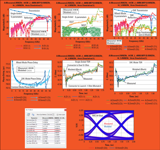
Figure 9 Example of detailed analysis to measurement correlation for 10 cm differential link in INNER6 - acceptable correlation up to 30 GHz, about 2 percent difference in modelled and measured eye diagrams.
An example of a detailed report for 10 cm differential stripline link in layer INNER6 is provided in Figure 9. We observed acceptable correspondence in the SE as well as in the mixed-mode S-parameters, to have less than 2 percent difference in the modelled and simulated 30 Gbps eyes. Substantial discrepancies above 30 GHz on all structures are caused by break out of the launch localization. The main reason for discrepancies in the reflections below 30 GHz is the variation of the impedance along the transmission line that is not accounted for in the model. We do not know what caused these variations, perhaps non-homogeneity of the materials or non-uniformity of the trace cross-sections or both. If so, it would be practically impossible to include all of those variations in the analysis because of a lack of the statistical distributions of the geometry and material parameters. A summary report for 10 structures is provided in Table 1.
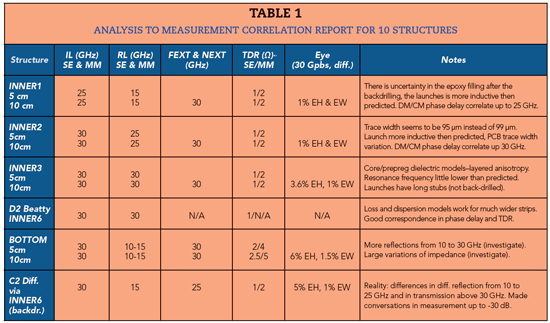
The first three columns of the table list acceptable correlation bandwidth for the insertion loss (IL), reflection loss (RL) and far- and near-end crosstalk (FEXT and NEXT). Column TDR shows the approximate absolute difference in computed and measured TDRs for SE and diff. modes. The TDR excludes the connector-to-launch transition area, where a 1.5/3 ohm difference was observed on all structures. The eye column shows the difference between the simulated and measured 30 Gbps NRZ eyes. Additional observations are listed in the “Notes” column. A complete report for all structures on the validation board is available on request.7
Conclusion
A systematic PCB interconnect analysis-to-measurement validation process is suggested and successfully used in this article. We outlined the minimal number of steps to have acceptable analysis-to-measurement correlation up to 30 GHz on most of the structures on the validation board. Technically, this is sufficient for the reliable analysis of 28 to 32 Gbps links. The design of launches and reference plane stitching localization degrades the correlation above 30 GHz. To extend the predictability up to 40 to 50 GHz, the launches have to be re-designed and manufacturing tolerances should be reduced.
The specificity of signal integrity problems also dictates very strict requirements for the measurement equipment - accuracy at low and high frequencies is equally important. The reality is that not all measurement equipment satisfies such requirements, and this is not common knowledge. Anyone with plans to purchase the equipment (or EDA tools) should try it first and evaluate S-parameters quality and validity, regardless of vendor. Validation boards are an excellent tool to do that. The selection of the measurement equipment and components caused substantial delay in this project.
We found that the identified dielectric parameters were very close to the vendor specs. Conductor roughness was the major contributor to signal degradation, no models were available in advance and analysis without proper conductor roughness models is useless. The Causal Huray-Bracken conductor roughness model provided good correlation in the losses and in the TDR impedance.
In conclusion, we should state that this is an ongoing project and we continue to investigate obtained data in preparation for the next validation board. We expect it will be actually predictable up to 40 GHz.
Acknowledgments: The authors gratefully acknowledge Ingvar Karlsson, Kunia Aihara, Davood Khoda, Kenneth Jonsson, Matti Nuutinen, Andreas Agerstig and Magnus Svevar for their valuable help during this lengthy project.
More detailed version of this article is available at www.signalintegrityjournal.com and this work was the basis of a Best Paper Award at DesignCon 2018.
[www.signalintegrityjournal.com/articles/1002]
References
- Y. Shlepnev, A. Neves, T. Dagostino, and S. McMorrow, “Measurement-Assisted Electromagnetic Extraction of Interconnect Parameters on Low-Cost FR-4 Boards for 6-20 Gb/sec Applications,” DesignCon 2009.
- D. Dunham, J. Lee, S. McMorrow, and Y. Shlepnev, “2.4 mm Design/Optimization with 50 GHz Material Characterization,” DesignCon 2011.
- Y. Shlepnev, “Sink or Swim at 28 Gbps,” The PCB Design Magazine, October 2014, pp. 12–23.
- W. Beyene, Y.C. Hahm, J. Ren, D. Secker, D. Mullen, and Y. Shlepnev, “Lessons learned: How to Make Predictable PCB Interconnects for Data Rates of 50 Gbps and Beyond,” DesignCon 2014.
- Y. Shlepnev, “Broadband Material Model Identification with GMS-Parameters,” IEEE 24th Conference on Electrical Performance of Electronic Packaging and Systems, 2015.
- Y. Shlepnev, Y. Choi, C. Cheng, and Y. Damgaci, “Drawbacks and Possible Improvements of Short Pulse Propagation Technique,” IEEE 25th Conference on Electrical Performance of Electronic Packaging and Systems, October 2016, pp. 141–143.
- M. Marin and Y. Shlepnev, “40 GHz PCB Interconnect Validation: Expectations vs. Reality,” DesignCon 2018.
- Y. Shlepnev, “Unified Approach to Interconnect Conductor Surface Roughness Modelling,” IEEE 26th Conference on Electrical Performance of Electronic Packaging and Systems, October 2017.