
The frequency content of digital signals in printed circuit board (PCB) interconnects increased up to 40 to 50 GHz in recent years. To ensure that interconnects work as expected over this bandwidth, we have to build validation boards. This article reports lessons learned from validation projects with the goal to build a formal procedure for systematic prediction of interconnect behavior up to 40 GHz.
What does it take to design PCB interconnects with good analysis-to-measurement correlation up to 40 GHz? Is it doable with typical low-cost PCB materials and fabrication process, typical trace width, via back-drilling, and the shortage of space to place the stitching vias? Your EDA vendor shows excellent correlation of the analysis tools to measurements even up to 50 GHz, your PCB fabricator ensures that the board will be built as designed and provides all possible information on stackup and materials. Measurements with the easy-to-use TDNA or VNA should be also a “piece of cake.” There is nothing to worry about and the designed interconnects should behave as expected.
Unfortunately, many SI engineers quickly learn that this is not the case and the reality can be far from our expectations. To verify practically everything that goes into the design-to-manufacturing flow at this frequency bandwidth, we are actually forced to build validation boards. Moreover, re-validation has to be done every time when a new material or fabricator is used. The outcome of such validation should be a formal process, which allows us to reduce the gap between expectations and reality, reliably predicting the behavior of the interconnects on production boards over this bandwidth. In this article, we do not just show the final analysis-to-measurement correlation on a case-by-case basis, but instead report a formal procedure based on the material model and manufacturing adjustments identification.
“Sink or Swim” Validation
A key element of design success is the systematic benchmarking of manufacturing, measurements, and modelling. Systematic means analysis-to-measurement correlation observed not just for one or two structures (test coupons for instance), but rather for a broad range of typical interconnects - single-ended (SE) and differential (diff.), stripline and microstrip, simple planar and with the vertical transitions or vias, etc. Such comparisons should be done consistently both in frequency (magnitude and phase of S-parameters) and time (TDR and optionally eye diagram) domains. In other words, systematic validation or benchmarking is needed to make sure that the board is manufactured as designed, measurements are taken properly and, finally, that the interconnect analysis software provides acceptable accuracy. It is a huge project. Fortunately, there are a number of reports about similar projects to follow.1-4 Here we will use the “sink or swim” approach.4 It can be divided into seven steps:
1. Select materials and define PCB stackup with the manufacturer.
2. Design test structures with an EM analysis tool (simple links, launches, vias, etc.).
3. Manufacture the board and mount the connectors.
4. Measure S-parameters and validate quality of the measurements with formal quality metrics and visual inspection.
5. Do a cross-section of the board and identify the manufacturing adjustments, if any.
6. Identify broadband dielectric and conductor roughness models with GMS-parameters or Short Pulse Propagation (SPP) light techniques.
7. Simulate all structures with the identified or validated material models and confirmed adjustments. Compare consistently S-parameters and TDR with the measurements (no further manipulations with the data or “calibration” are allowed at this step).
The next sections of this paper outline the selection of the materials and board design with the stackup structure close to a typical production board. We then describe the measurement process, board cross-sectioning material parameters identification, and, finally, see how close to the reality we can get by following the process.
Validation Board
A validation platform, whether developed in house or purchased, is very important to pre-qualify a manufacturer, benchmark signal integrity software or learn how to do measurements in the microwave to mmWave bandwidths. The accuracy and limitations of the software can be easily identified with analysis-to-measurement comparisons on a typical set of interconnect structures. One of the first validation platforms was the physical layer reference design board (PLRD-1) from Teraspeed Consulting Group.1 An example of a readily available validation platform is the CMP-28/32 channel modelling platform from Wild River Technology.3
Off-the-shelf validation platforms are convenient, but their stackup and interconnect geometry may not be representative for a production board. So, custom validation platforms with a stackup structure similar to a production board have to be used, as is done in this project. The board design starts from the material selection and stackup definition. We selected Panasonic Megtron6 material for the high speed routing layers. The board has 20 layers with eight layers assigned for high speed signals (see Figure 1). The target impedance has been specified for the PCB manufacturer who has to fulfill it with eight percent tolerance. That is too large variation to expect good correlation even up to 40 GHz, but this is the typical choice for a production board. The manufacturer also provided expected trace widths and spacing adjustment. The stackup for the pre-layout analysis was defined (see right side of Figure 1). Megtron6 specs provide dielectric constant and loss tangent at multiple frequencies. It is expected that the Wideband Debye (aka Djordjevic-Sarkar) model (defined using the specs) provides a good approximation over the target frequency bandwidth.
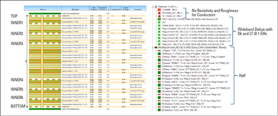
Figure 1 Validation board stackup (left) and the initial material models in Simbeor software (right).
In Figure 1, the values for Dk are the ones used by PCB manufacturer based upon their experience with this material. The major problem is with the conductor roughness model: the copper foil roughness is specified as H-VLP and no other data. PCB manufacturers also roughen the shiny side of the copper foil during board manufacturing, without any parameters for the electrical modelling. So, even if we had data for the matte side of the copper foil, the PCB manufacturer treatment of the shiny side would make it practically useless. Thus, we start without the conductor roughness model and with the trace adjustments provided by the PCB manufacturer. The structures on the validation board, then, should be useful for material model identification/validation. For identification with GMS-parameters5 or SPP Light6, we used two segments (5 and 10 cm) of differential or SE transmission lines for each unique layer. We also used the Beatty standard (series resonator) to confirm that the extracted models work for traces with different widths. The line segments used for material identification can also be used as tests for simple diff. and SE links (they are similar to the traces used on production boards). In addition, we decided to use structures typically used in interconnects for the serial and parallel interfaces: diff. and SE via-holes for each routing layer; AC coupling capacitors similar to used on SERDES links; meandering line segment similar to used on DDR links; and diff. link skew compensation structures. All are routed at an angle to the edge of the board to avoid the fiber weave effect. The final board layout with all structures is shown in Figure 2.
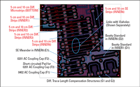
Figure 2 Layout of 20 layer validation board. Red legends are for the material identification structures.
The launches are the most important elements of the validation board design, and they have to be optimized. If they reflect too much, they will likely be more susceptible to manufacturing variations and more difficult to de-embed for the material identification. The validation board was designed to have either 2.92 or 2.40 mm compression-mount connectors mounted on the TOP layer. We used connectors from two vendors. Five low-reflection launches were designed to connect the TOP and BOTTOM for structures with microstrip lines, TOP to INNER1, 2, 3 (with back-drilling), and TOP to INNER6 (with small stubs). Stackup/materials obtained from the manufacturer were used to simulate and optimize the launches, and they were designed to be functional up to 30 GHz.
At the end of the board layout phase we noted the following issues, which make the post-layout analysis inaccurate and practically useless for the target bandwidth:
- The PCB is manufactured with the “impedance control” process - all trace width and spacing adjusted by the PCB manufacturer must be accounted for in the post-layout analysis.
- No information on trace shape (etching).
- Ask shape/parameters.
- No information on conductor roughness model.
- No information on actual backdrilling.
Measurements and GMS-Parameters
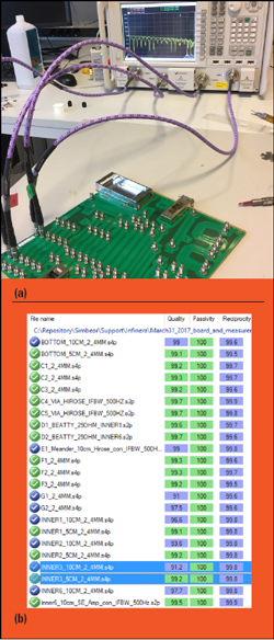
Figure 3 S-parameters measurement setup with 50 GHz VNA (a) and final Simbeor quality metrics (b), the metrics are in the process of standardization by IEEE T370 PG3.
The main goal during the measurement step is to have accurate high-quality S-parameters measured from 10 MHz to 40 GHz. Also, the S-parameters should be suitable for the extraction of the reflection-less GMS-parameters for material parameters identification5 up to 30 GHz. Achieving this goal was the most challenging step in the project.
The board was manufactured as scheduled, and the S-parameters were measured first with TDNA. The formal quality metrics of these S-parameters was barely acceptable. Though, the visual inspection revealed a lot of noise in the S-parameters magnitudes. The GMS-parameters5 computed with these S-parameters were also very noisy and considered not acceptable for the material identification. If we would proceed with the noisy GMS-parameters, the material identification becomes ambiguous above 10 GHz. Thus we decided to find other measurement options. For instance, we used a 26 GHz VNA, multiple 40 GHz VNAs and one 50 GHz VNA.
The final measurement setup with 50 GHz VNA is shown in Figure 3. The measurements came out with the high formal quality metrics as shown on the bottom of the Figure 3. However, a closer look at the lower frequencies revealed a problem: the reflection parameters converge to incorrect values at frequencies below 70 MHz. The VNA vendor explained this as the defect of the electronic calibration kit. To overcome the problem and be able to identify conductor resistivity, we did additional measurements with a mechanical calibration kit, but it had lower bandwidth and was used for the resistivity identification only.
In regards to measurements, we stress that broadband measurements of S-parameters for signal integrity purposes are particularly challenging, and not all measurement equipment is suitable. SI problems require high accuracy over extremely broad bandwidth. Though at this step, the GMS-parameters are successfully extracted up to 30 GHz, which is sufficient to identify the frequency-continuous material models that are expected to work up to 40 to 50 GHz. Also, measurements down to 10 MHz are available to identify the copper resistivity.
Board Cross-Sectioning
Before material parameters identification, we had to know the actual geometry of the traces for the material identification structures. As was observed in a similar project,4 the actual geometry can be very far from expected, so the resulting analysis results can be unreliable.
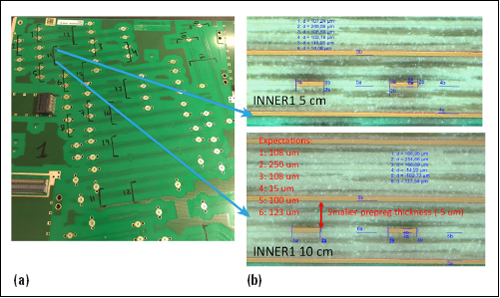
Figure 4 Validation board cross-sectioning plan (a) and example of the cross-sectioning analysis for 5 and 10 cm links in layer INNER1 (b).
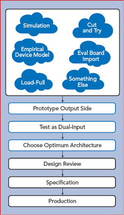
Figure 5 Cross-sectioning analysis for 5 and 10 cm links in layer INNER6 (a) and in layer BOTTOM (b), large differences.
Traces on the material identification structures, launches, Beatty in INNER6, and some viaholes have been cross-sectioned as shown in Figure 4. This is not a statistical investigation but rather validation of our expectations based on the adjustments provided by the manufacturer. Analysis of the cross-sections of traces in layers INNER1 is shown in Figure 4 on the right. Analysis of the cross-sections in layer INNER6 and BOTTOM is shown in Figure 5.
The first observation is that the prepreg layer thickness is 3 to 5 μm thinner than provided by the manufacturer (expectation column in Figures 4 and 5). With that adjustment, the thickness of the interior prepreg layers becomes closer to the thickness of the core layer. The second observation is that the geometry of the stripline traces are very close to the expectations. Even without the cross-sectioning, the material identification and analysis results would be very close. Though, it is totally different for the microstrips as we can see in Figure 5. The final trace width and distance adjustments are summarized in Figure 6. The most critical adjustments for the microstrips are highlighted in red. The microstrip metal layer thickness is 48 μm instead of the expected 35 μm, and the solder mask layer has a thickness of 10 μm over the strips and 38 μm between the strips (that was not known in advance). The analysis with the microstrip geometry from the board layout or even with the adjustments obtained from the manufacturer would lead to characteristic impedance mismatch, about 3 ohm for the SE and about 6 ohm for the diff. microstrip traces. We can state that the analysis with the trace width and spacing specified in the original layout are not acceptable to provide good accuracy even below 10 GHz due to considerable impedance mismatch. The microstrip trace adjustments cannot be predicted and properly accounted for without the cross-sectioning. Though, the adjustments provided by the board manufacturer for stripline layers can be safely used. In addition to traces, some viaholes marked in Figure 4 were cross-sectioned and compared with the expectations: the results are available in the complete report.7 At this point, everything is ready for the material models identification.
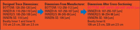
Figure 6 Width-distance-width adjustments for the differential traces and width adjustment for SE traces (can be applied only for the impedance controlled segments).