
This article reports the experimental evaluation of a 0.24-µ m CMOS technology for Bluetooth power applications. From load-pull measurements, the 0.24-µ m CMOS power transistor can deliver 23 dBm output power with 39 percent PAE at 2.4 GHz. A modified BSIM3v3 RF model with a new substrate network is presented for the design of Bluetooth power amplifiers. The simulation results of the proposed model show better agreement with the S-parameter and load-pull measurement results than several previously reported BSIM3v3 RF models.
Bluetooth technology, an emerging short-range wireless application at the unlicensed 2.4-GHz industrial, scientific and medical (ISM) band,1 has drawn lots of attention recently because of the potentially huge commercial market. In addition to replacing many proprietary cables, Bluetooth technology also provides a universal bridge to the existing data networks, a peripheral interface, and a mechanism to form small private ad hoc groupings of connected devices away from fixed network infrastructures. However, one of the key requirements for Bluetooth technology to prevail is the supply of low cost and compact transceivers.
CMOS technology leverages the existing digital very large scale integration (VLSI) technology and benefits from mixed-signal IC development. Through scaling to reduce the channel length, CMOS transistors continue to improve their fT and minimum noise figure Fmin . Due to these advances, many RF transceiver building blocks, such as low noise amplifiers2,3 and mixers,4,5 have been demonstrated with the commercially available deep sub-micron CMOS technology. However, for RF power amplifier implementation, more device characteristics other than high fT and low Fmin must be considered. Linearity, efficiency and power handling capability are also major concerns of power transistor characteristics.
Although the low drain-source breakdown voltage limits deep sub-micron CMOS technology in high power applications, the maximum transmission power of Bluetooth technology requires only 20 dBm. The low output power of Bluetooth technology facilitates the low voltage operation and relieves the low breakdown voltage of the deep sub-micron CMOS devices. In addition, the constant-envelope Gaussian frequency shift keying (GFSK) modulation scheme of the Bluetooth standard relaxes the linearity requirements and allows the power transistors to be driven in the nonlinear regime for efficient operation.
This article reports the feasibility evaluation of a 0.24-µm CMOS technology for Bluetooth power applications. In addition to DC and high frequency S-parameter measurements, load-pull measurements are used to investigate the power performance of the deep sub-micron CMOS technology. A modified BISM3v3 model with a new substrate network is proposed for the design of RF power amplifiers. Although several modified BSIM3v3 models have been reported, these models are validated with only small-signal S-parameters. Small-signal models are not adequate for the circuit simulations of RF power amplifiers because of large-signal swings. To the authors' knowledge, the proposed model demonstrates for the first time that the BSIM3v3 RF model is capable of accurate RF small-signal and large-signal simulations.
TECHNOLOGY
The 0.24-µm p-substrate twin-well CMOS technology is similar to most commercial digital deep sub-micron CMOS technology. The sheet resistance of the Si substrate is approximately 10 Ω-cm. There are five metal layers for flexible interconnection. The gate poly is salicided to reduce the gate resistance and transistor noise. In addition to the gate poly, the second poly layer is available for the implementation of poly-oxide-poly capacitors. The total gate width of the NMOS power transistor under investigation is 2000 µm (40 * 50 µm). The transistor has an interdigitated layout with 40 gate fingers and 50-µm width for every gate finger.
EXPERIMENTAL EVALUATION
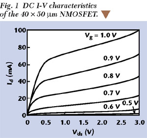
The I-V characteristics of the NMOS power transistor from DC measurement are shown in Figure 1. The gate voltage Vgs sweeps from 0.5 to 1.0 V with 0.1 V steps. No significant current crush effects (as often described in III-V devices) are observed due to the superior thermal conductivity of the silicon substrate. For Vds = 2.5 V and Vgs = 0.9 V the transconductance gm is 139 mS/mm. The measured drain-source breakdown voltage Vdso is 5.4 V.
The high frequency S-parameter data is measured at Vds = 2.5 V and Vgs = 1 V. The probe pad effects are de-embedded by use of an open test structure. The current gain and maximum available gain Gmax are shown in Figure 2. The fT and fmax of the transistor are 25 GHz and 11 GHz, respectively. It is not unusual to observe higher fT than fmax for a CMOS power transistor because the fT and fmax of a MOS transistor are related as

where
|
Rg |
= |
gate resistance | |
|
Cgd |
= gain-drain capacitance6 |
| |

Since both Rg and Cgd are proportional to the single gate width of a MOSFET, the fmax of a large MOSFET could be lower than its fT .
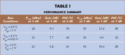
Load-pull measurement is used to evaluate the power capability of the 40 * 50-µm NMOSFET at 2.4 GHz. The load contour of constant output power for the 12-dBm input power is shown in Figure 3. The device is biased at Vds = 2.5 V and Vgs = 1 V. The source impedance is conjugate-matched to the device input impedance. The measured maximum output power is 21.8 dBm with the load at 0.72  176° on the Smith chart. As the load impedance is tuned for maximum output power, the measured output power, power-added efficiency (PAE) and power gain with respect to input power are shown in Figure 4. When the input power is 14 dBm, the NMOSFET can deliver 23 dBm output power with 39 percent PAE. At the class-B bias condition Vds = 2.5 V and Vgs = 0.55 V, the output power drops to 21 dBm, but the PAE rises to 42 percent as expected. For low voltage operation, the Vds can be reduced to 2 V. At Vds = 2 V and Vgs = 1 V, the measured output power and PAE are 22 dBm and 42 percent, respectively. The low voltage operation presents higher power gain than class-B operation for the NMOS power transistor. In general, class-B operation delivers the highest efficiency of these three operation modes, but the low voltage operation can also achieve about the same efficiency when the transistor is driven by high input power. The output power, power gain and PAE at the 1 dB and 3 dB compression points under these three bias conditions are listed in Table 1.


BSIM3v3 RF MODELS
Having demonstrated scalability and accuracy in device I-V and low frequency characteristics, the BSIM3v3 model has become an industry standard for deep sub-micrometer MOSFETs. However, BSIM3v3 is still not capable of modeling the RF characteristics of deep sub-micron MOS transistors. Figure 5 shows the simulation results of the BSIM3v3 model and measured S-parameter data of the 0.24-µm NMOS power transistor from 100 MHz to 8 GHz. The transistor is biased at Vds = 2.5 V and Vgs = 1 V. The gain predicted by the BSIM3v3 model is overestimated, and the input and output impedances also deviate from the measured data. Because impedance matching is crucial to the performance of RF circuits, the present BSIM3v3 model is inadequate for RF circuit designs. The comparison of load-pull simulation with the BSIM3v3 model and load-pull measurement is shown in Figure 6. Both the simulated output power and PAE are much higher than the measured results under the same load impedance.


In order to extend the application of the BISM3v3 model to RF, the effects that should be included in the modeling79 include distributed channel or non-quasi-static (NQS) effects, distributed gated resistance and distributed substrate parasitics.
Recent papers710 addressed these issues by adding lumped elements on top of the BSIM3v3 model. Gate resistors are added in all of the modified BSIM3v3 RF models to account for NQS effects and fit the S11 . Moreover, the gate resistor can also be used to model the gate-induced thermal noise.11 Although BSIM3v3 has the option to enable the non-quasi-static mode (NQSMOD = 1) and define the Elmore delay, previous research shows that adding a gate resistor models the input impedance more accurately at RF.9 The reported BSIM3v3 RF models are summarized as follows:
* Model of Liu et al.7 as shown in Figure 7(a): The transistor junction areas and junction peripheries in the BSIM3v3 model, AS , AD , PS and PD are set to zero. The drain-bulk junction capacitance Cjdb and source-bulk junction capacitance Cjsb are included in the lumped-element substrate network outside the BSIM model.

* Model of Ou et al.8 as shown in Figure 7(b): The parameters of transistor junction areas and peripheries are also set to zero. The substrate networks are simplified as series RC networks connecting to the drain and source. The substrate networks are simple, but this model has difficulties in fitting Y12 and Y22 at RF.9
* Model of Tin et al.9 as shown in Figure 7(c): The parameters of transistor junction areas and peripheries are not set to zero. The p-n junction diode and parasitic capacitances built-in the BSIM3v3 model are used with the substrate network. Since the bias dependence is captured in the built-in capacitance model, no separate capacitance extractions are required. Therefore, the substrate is modeled simply by a resistor connecting to bulk.
* Model of Lee et al.10 as shown in Figure 7(d): Based on the Tin model9 , the external drain-bulk and source-bulk junction capacitances are added in the substrate network to improve the model accuracy and dispersion effect in the effective drain-source resistance and capacitance.
Since the Tin model9 is comparatively simpler and more accurate than the modified BSIM3v3 models reported in Liu7 and Ou,8 only the models of Tin9 and Lee10 are extracted and compared with the proposed new BSIM3v3 RF model as shown in Figure 8. Because the output impedance of a transistor is critical to the RF power performance, the new model utilizes the parasitic capacitances built in the BSIM3v3 and the substrate network of five lumped elements to model S22 more accurately.

MODEL VALIDATION
The small-signal RF behavior of the modified BSIM3v3 models is verified with measured S-parameters from 100 MHz to 8 GHz as shown in Figure 9. The bias condition for the measurement and simulation is Vds = 2.5 V and Vgs = 1 V. In general, all of the BSIM3v3 RF models under investigation present the RF characteristics of the deep sub-micron MOSFET much more accurately than the BSIM3v3 model. From the data, it is observed that the simulation results of the models reported in Tin9 and Lee10 are very similar. However, the proposed new model offers more freedom to fit the measured S-parameters, especially S22 . The differences between the models of Tin9 and Lee10 are the explicit substrate junction capacitors, Cjdb and Cjsb . As the implicit junction capacitances built-in BSIM3v3 have been modeled very well, the added explicit capacitors in the model of Lee10 cannot result in significant improvement.

For RF power applications, the transistor models cannot be validated with only small-signal S-parameters. The large-signal characteristics of the transistors should also be incorporated in the models for accurate circuit simulations. Therefore, the large-signal behaviors of the BSIM3v3 RF models under investigation are simulated with a harmonic balance simulator. The bias conditions and matching impedances of the simulation are set up the same as the measurement. Figure 10 shows the modeled output power versus input power at 2.4 GHz. The proposed new model predicts the output power more accurately than the other two models. The simulated PAE of the new model also matches the measured PAE for every input power level. The model of Tin9 is in agreement with the measured output power, but it underestimates the PAE at high input power levels. From the large-signal validation results, the proposed new BSIM3v3 RF model demonstrates its capability for RF power applications.

CONCLUSION
A 0.24-µm CMOS technology has been evaluated for Bluetooth power applications. The 0.24-µm NMOS power transistor of 40 * 50µm gate width can deliver 23 dBm output power with 39 percent PAE at 2.4 GHz. The fT and fmax of the power device are 25 GHz and 11 GHz, respectively. From the DC I-V, S-parameter and load-pull measurement results, the 0.24-µm CMOS technology is feasible for Bluetooth power amplifier implementation. A new BSIM3v3 RF model is compared with several previously reported models. In addition to small-signal S-parameter data, the new model is also verified with the large-signal load-pull data. The good agreement between the simulated and measured results demonstrates that the new BSIM3v3 RF model can be used for Bluetooth power amplifier design.
ACKNOWLEDGMENT
This work was partially supported by grants from the Office of Naval Research and the National Science Foundation. The material for this article was first presented at the RAWCON2000 IEEE Radio and Wireless Conference held in Denver, CO in September 2000. *
References
1. "Wireless Personal Area Networks: An Overview," Monday Workshop Notes, 1999 IEEE Radio and Wireless Conference, Denver, August 1999.
2. Q. Huang, P. Orsatti and F. Piazza, "Broadband, 0.25 µm CMOS LNAs with Sub-2 dB NF for GSM Applications," Proceedings of the IEEE Custom Integrated Circuits Conference, May 1998, pp. 6770.
3. D. Shaeffer and T. Lee, "A 1.5 V, 1.5 GHz CMOS Low Noise Amplifier," IEEE Journal of Solid-state Circuits, Vol. 32, No. 5, May 1997, pp. 745759.
4. P. Sullivan, B. Xavier and W. Ku, "Doubly Balanced Dual-gate CMOS Mixer," IEEE Journal of Solid-State Circuits, Vol. 34, No. 6, June 1999, pp. 878881.
5. F. Piazza and Q. Huang, "A High Linearity, Single-ended Input Double-balanced Mixer in 0.25 µm CMOS," Proceedings of 24th European Solid-State Circuits Conference, September 1998, pp. 6063.
6. T. Manku, "Microwave CMOS - Device Physics and Design," IEEE Journal of Solid-State Circuits, Vol. 34, No. 3, March 1999, pp. 277285.
7. W. Liu, R. Gharpurey, M.C. Chang, U. Erdogan, R. Aggarwal and J.P. Mattia, "RF MOSFET Modeling Accounting for Distributed Substrate and Channel Resistances with Emphasis on the BSIM3v3 SPICE Model," IEEE IEDM-97 Digest, December 1997, pp. 309312.
8. Jia-Jiunn Ou, Xiaodong Jin, Ingrid Ma, Chenming Hu and Paul Gray, "CMOS RF Modeling for GHz Communication ICs," 1998 VLSI Technology Symposium Digest, June 1998, pp. 9495.
9. Suet Fong Tin, Ashraf Osman, Kartikeya Mayaram and Chenming Hu, "A Simple Subcircuit Extension of the BSIM3v3 Model for CMOS RF Design," IEEE Journal of Solid-State Circuits, Vol. 35, No. 4, April 2000, pp. 612624.
10. Seonghearn Lee, Cheon Soo Kim and Hyun Kyu Yu, "A RF MOSFET SPICE Model with a New Substrate Network," Proceedings of the IEEE RAWCON 2000, September 2000, pp. 203206.
11. Xiaodong Jin, Jia-Jiunn Ou, Chih-Hung Chen, Weidong Liu, M. Jamal Deen, Paul R. Gray and Chenming Hu, "An Effective Gate Resistance Model for CMOS RF and Noise Modeling," IEEE Internal Electron Device Meetings Digest, December 1998, pp. 961964.
 Yi-Jan Emery Chen received his BS degree in electrical engineering from National Taiwan University, Taipei, and his MS degree in electrical engineering from the University of California at Santa Barbara. Previously, he had been with Siemens Telecommunication Systems Ltd. and Tektronix Taiwan Ltd. Currently he is pursuing his PhD degree at the Georgia Institute of Technology, Atlanta. Since 1998, he has been working as a co-op with National Semiconductor's Wireless Communication Group. His research interests include RF integrated circuit design, device modeling and MCM development in CMOS, BiCMOS and SiGe technology for wireless applications.
 Deukhyoun Heo received his BSEE degree in electrical engineering from Kyoungpuk National University, Daegu, South Korea, in 1989 and worked as a senior engineer in LG Information and Communications Ltd. for six years. In 1997, he received his MSEE degree in electrical engineering from Pohang University of Science and Technology (POSTECH), Pohang, South Korea. Currently, Heo is pursuing his PhD degree at the Georgia Institute of Technology, Atlanta. His research interests include microwave devices and circuits and their applications. He has primarily been concerned with RF/microwave transceiver design based on CMOS, BiCMOS, SiGe and GaAs technologies for wireless communications, the development of active device nonlinear model for power amplifier and the multi-layer module development based on MCM-C technology. Heo is the recipient of the IEEE MTT IMS 2000 Best Paper award.
 Dr. Joy Laskar received his BS degree from Clemson University in 1985. Prior to joining Georgia Tech in 1995, Dr. Laskar held faculty positions at the University of Illinois and the University of Hawaii. At Georgia Tech, he is currently the chair for the Electronic Design and Applications technical interest group, the Yamacraw Research Leader for Broadband Access Hardware and the Packaging Research Center thrust leader for RF and Wireless. His research has focused on high frequency IC design and their integration. At Georgia Tech, Dr. Laskar heads a research group of 20 members with a focus on integration of high frequency electronics with optoelectronics and integration of mixed technologies for next generation wireless and optoelectronic systems. Dr. Laskar's research is supported by over 15 companies and numerous federal agencies including DARPA, NASA and NSF. He is a co-organizer and chair for the Advanced Heterostructure Workshop, serves on the IEEE Microwave Theory and Techniques Symposia technical program committee, and is a member of the North American Manufacturing Initiative roadmapping committee. Dr. Laskar has published over 100 papers, has participated in numerous invited talks and has eight patents pending. He is a 1995 recipient of the Army Research Office's Young Investigator Award, a 1996 recipient of the National Science Foundation's CAREER Award, the 1997 NSF Packaging Research Center Faculty of the Year, the 1998 NSF Packaging Research Center Educator of the Year, the 1999 recipient of the IEEE Rappaport Award (Best IEEE Electron Devices Society Journal Paper), the 2000 recipient of the IEEE MTT IMS Best Paper award, and is co-founder and Director of a Broadband Wireless Company called RF Solutions.
Dave Bien received his BSEE degree from Lehigh University and his MEng from Cornell University. He has been active in semiconductor and IC development since 1979, and holds several patents related to circuit and device design. His interests are in analog and RF integrated circuits. Previously, he had been employed with National Semiconductor's Wireless Communications Group. He is currently with Motorola's Semiconductor Products Sector.