
Wideband CDMA (W-CDMA) is one of several digital cellular technologies that is competing for the third generation (3G) cellular market. The earlier Japanese W-CDMA trial system and the European Universal Mobile Telephone System (UMTS) have each served as a foundation for the workings of this harmonized W-CDMA system under the supervision of the Third Generation Partnership Project (3GPP). The harmonized system is commonly referred to as 3GPP W-CDMA, to distinguish it from earlier wideband CDMA versions.
The 3GPP W-CDMA system will employ W-CDMA in both frequency division duplex (FDD) and time division duplex (TDD) modes. As a 3G technology, W-CDMA must support variable data rates to accommodate both voice and high data rate applications (for example, video and packet data). The W-CDMA specifications use the term user equipment (UE) to refer to mobile phones, wireless computer devices, or other devices that provide wireless access to the W-CDMA system. Unlike second generation (2G) CDMA mobile stations, the W-CDMA UE can transmit more than one code channel in order to accommodate the high data rates. The UE behaves, in essence, as a miniature CDMA base transceiver station (BTS). As with a CDMA BTS, it is important to analyze the code-by-code composition of the W-CDMA UE signal in order to characterize and troubleshoot the transmitter. This article describes the code domain structure of W-CDMA uplink (UL) signals and explains how the different code domain analysis measurements can be used when developing and troubleshooting a W-CDMA UE transmitter. Throughout this article, the term W-CDMA refers to the 3GPP W-CDMA (Release 99) FDD mode.
UPLINK AIR INTERFACE
In W-CDMA, the user's digitized voice and data channels, along with signaling data from higher protocol layers, are carried in the dedicated physical data and control channels (DPDCH/DPCCH). The payload data and signaling data channels (DPDCH) are transmitted on the I path of the QPSK modulator; the power control, pilot and other overhead bits (DPCCH) are transmitted on the Q path.
A single UE can transmit several DPDCHs in order to obtain higher data rates. In this case, they are consecutively assigned to either the I or Q path. Each DPDCH/DPCCH is spread by a channelization code, also known as orthogonal variable spreading factor (OVSF) code, and its amplitude can be individually adjusted.
OVSF codes are orthogonal codes similar to the Walsh codes used in 2G CDMA (IS-95) BTS. Each channel originating from a W-CDMA UE is multiplied by a different OVSF code. In IS-95 BTS, Walsh codes were fixed at 64 chips in length; in W-CDMA, the length of the codes, also known as the spreading factor (SF), is variable. For UL, the SF can be 4, 8, 16, 32, 64, 128 or 256, corresponding to DPDCH bit rates from 960 kbps down to 15 kbps. For example, a DPDCH with a bit rate of 60 kbps will be spread by an OVSF code with a SF of 64, as shown in Figure 1. The bit rate for the DPCCH is fixed at 15 kbps. The spread data rate, known as the chip rate, is fixed at 3.84 million chips-per-second (Mcps).

As in other CDMA systems, each UE (and BTS) composite spread signal is scrambled by a unique pseudo-noise (PN) scrambling code. This code is used by the BTS to identify the UE.
In the case of the W-CDMA UE, the scrambling code is a special complex function that limits the signal transitions across the origin of the IQ plane and also reduces the 0° phase shift transitions. This function improves its peak-to-average power ratio. The function can be considered a variation of regular complex scrambling and is commonly known as hybrid phase shift keying (HPSK), although this term is not mentioned in the standard. The scrambling generator produces two random sequences (referenced in the standard as Clong,1 and Clong,2 if long scrambling sequences are used1 ). The second sequence is decimated, multiplied with the function {1,1} and, with the first sequence, applied to the Q path of the complex scrambler. The first sequence is also applied to the I path of the complex scrambler. For a more detailed description of HPSK refer to Application Note 13352 . The resulting I and Q signals are then filtered and used to modulate the RF carrier (not shown in the figure).
The combination of OVSF codes and scrambling codes provides the signal spreading, and therefore the spreading gain needed for the receiver correlators to pull the desired signal out of the noise. The SF determines the degree of spreading gain. For high data rate signals, the SF and spreading gain are lower. For the same level of interference, the amplitude for high data rate channels must be higher in order for all channels to maintain equal energy-per-bit-to-noise ratio (Eb /No ).
CODE DOMAIN POWER
Many measurements are available to analyze the modulation accuracy of a UE transmitter: quadrature phase shift keying (QPSK); error vector magnitude (EVM); composite EVM; code domain power and symbol EVM.3 Selecting the appropriate measurement depends on many factors, including the stage of development of the UE and the specific objectives of the engineer performing the measurement. The primary means of investigating the code-by-code composition of the signal is to observe the distribution of power in the code domain.
Code domain power is an analysis of the distribution of signal power across the set of code channels, normalized to the total signal power. To analyze the composite waveform, each code channel is decoded using a code-correlation algorithm. This algorithm determines the correlation coefficient factor for each code. Once the channels are decoded, the power in each code channel is determined.
Code domain power was already used to analyze the code composition of IS-95 BTS. In W-CDMA, the measurement is complicated by the fact that the SF varies to accommodate the different data rates. As the user rate increases, the bit period is shorter. Since the final chip rate is constant, fewer OVSF code chips are accommodated within the bit period -- the SF is smaller.
Seven sets of spreading codes are specified, one set for each spreading factor (4, 8, 16, 32, 64, 128 or 256). The OVSF codes can be allocated using the code tree shown in Figure 2. Each code is denoted by Cch,SF,n . For example, Cch,4,2 means channelization code SF = 4 and code number 2.
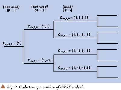
In this tree, OVSF codes of a certain SF are obtained by copying the mother-branch code of the previous SF, and repeating or inverting it. For example, Cch,4,2 = (1,1,1,1) is obtained by copying and repeating Cch,2,1 = (1,1), while Cch,4,3 = (1,1,1,1) is obtained by copying Cch,2,1 = (1,1) and inverting it. This code generation technique is known as the reverse-bit method.
One of the consequences of using variable SFs is that a shorter code precludes using all longer codes derived from it. Figure 3 shows this concept. If a high data rate channel using a code of SF = 4, for example, 1,1,1,1 is selected, all lower data rate channels using longer OVSF codes that start with 1,1,1,1 have to be inactive, because they are not orthogonal.

For UL, the physical channels are I/Q multiplexed. A special scrambling function (HPSK) is applied to limit the peak-to-average power ratio. However, HPSK limits the choice of OVSF codes. In order to benefit from HPSK, the OVSF codes must consist of pairs of consecutive identical chips.2 For example, Cch,4,1 = (1,1,1,1) would meet this condition, but Cch,4,2 = (1,1,1,1) would not.
Careful choice of OVSF codes can lead to lower peak-to-average power ratios. Exhaustive simulations using complementary cumulative distribution function (CCDF) curves led to the following standard specifications for the OVSF codes1 :
* The DPCCH is always spread by code Cch,256,0 = (1,1,1,1,1,......);
* When only one DPDCH is to be transmitted, it is spread by code Cch,SF,SF/4 = (1,1,1,1,1,1, 1,1.....);
* When more than one DPDCH is to be transmitted (because of high data rates), all DPDCHs have spreading factors equal to 4. Two DPDCHs can share the same code, since one would be in I and the other in Q, which makes them orthogonal. The channelization codes for the DPDCHs are defined as: Cch,4,1 = (1,1,1,1) for the 1st and 2nd DPDCHs; Cch,4,3 = (1,1,1,1) for the 3rd and 4th DPDCHs; and Cch,4,2 = (1,1,1,1) for the 5th and 6th DPDCHs.
Even though the OVSF codes were selected to maximize the benefits of HPSK, the HPSK requirements would be completely fulfilled only for the first two DPDCHs. The worst case of peak-to-average power ratio would be when five or six channels are required to cover the high data rates. It is expected that this condition will only occur in a very low percentage of cases. However, this does not make solving the problem easier for the amplifier designer.
In terms of code capacity, channels with higher data rates (lower SF) occupy more code space. For example, Cch,4,1 occupies four times more code space than Cch,8,2 , and sixteen times more code space than Cch,16,4 . The wider bars in the code domain power display represent codes with low SF that occupy more of the code space. Figure 4 shows the code domain power display for a signal with a DPCCH and 3 DPDCHs. The 3 DPDCHs (at 960 kbps, SF = 4) are much wider than the DPCCH (at 15 kbps, SF = 256). In order to provide this display, the analyzer must be able to identify the SFs of the code channels being measured.

The code domain power measurement helps not only to verify that each OVSF channel is operating at its proper amplitude, but also to identify problems throughout the transmitter design, from the coding to the RF section. In particular, the levels of the inactive channels can provide useful information about specific impairments. Ideally, the level for the inactive channels would be zero. In reality, signal and system imperfections compromise the code orthogonality and result in a certain amount of the signal power projecting onto inactive codes. A real signal will also have a certain noise level which, being random, will project more or less evenly onto all codes.
The projection of the error is interesting because it demonstrates how the error power is distributed in the code domain. It is desirable to have the error power evenly distributed through the code domain, rather than concentrated in a few codes, to avoid code-dependent channel quality variations.
One possible cause of non-equal distribution of error power is LO instability. In essence, energy is lost from the active channels and appears in those channels with codes that are closely related to the active channel codes.4 In the case of OVSF codes, this results in higher code domain noise for channels with code assignments consecutive to the active channel code. Channels with the same code assignment as the active channels, but applied in the opposite I/Q path, will also be affected, as shown in Figure 5.

PEAK CODE DOMAIN ERROR
As in other digital communication systems, the W-CDMA standard specifies an EVM measurement (composite EVM) as the modulation accuracy test.3,5
In W-CDMA, specifically to address the possibility of uneven error power distribution, the composite EVM measurement has been supplemented by another test called peak code domain error, which specifies a limit for the error power in any one code.5
To provide this metric, the analyzer must project the error vector power on each code channel at a SF of 256. The peak code domain power is then calculated from the code that returns the largest error power relative to the reference.
Gaussian noise distributes the power evenly through the code domain. By contrast, transmitter impairments typically cause the highest code domain errors in the active code channels, since the code domain energy lost from these channels (their code domain error) is usually spread in several code channels. Figure 6 shows the peak code domain error, in combination with the composite EVM3 , for the same signal with the described LO instability problem. In this case, the peak code domain error is at OVSF code 65 at SF = 256 (Cch,256,65 ) in I. This corresponds to OVSF code 32 at SF = 128 (Cch,128,32 ) in I, since Cch,128,32 maps onto codes Cch,256,64 and Cch,256,65 . The measurement display also shows the peak code domain error over all the active channels. In this case, the peak active code domain error belongs to the DPDCH (Cch,128,32 ). This error (14.65 dB) is larger than the peak code domain error at Cch,256,65 (16.17 dB) because of the error power contribution of Cch,256,64 .

Apart from looking at the code domain power and peak code domain error, it may be useful to analyze a specific code channel. The following sections describe some analysis tools and how they can be applied. Figure 7 shows how these measurements are calculated.

SYMBOL EVM
By de-scrambling and de-spreading the signal, the constellation for a specific code channel at the symbol level can be analyzed, even in the presence of multiple code channels. The measured signal is complex de-scrambled, de-spread and binary phase shift keying (BPSK) decoded to bits. The ideal bits are then BPSK encoded to obtain the reference at the symbol level. This reference is compared to the measured de-spread symbols.3
An RF impairment that affects symbol EVM will also affect the composite EVM, which provides a measure of modulation quality for the composite signal at the chip level.3 For example, an amplifier compression problem would appear both in the composite EVM and in the symbol EVM measurement. However, because of the spreading gain, symbol EVM will mute the impairment. So why use symbol EVM?
Symbol EVM provides the bridge between RF and the demodulated bits. Since it includes the spreading gain, it provides baseband engineers with a measure of modulation quality that is closer to real life performance. In this sense, it can be thought of as the actual quality that the user will experience in that channel (similar to the reciprocal of bit error rate (BER)).
The relationship between symbol EVM and chip EVM depends on the SF. For low SFs (less spreading gain), chip modulation errors have a significant effect on symbol EVM, but for high SFs (more spreading gain), chip modulation errors have very little effect on symbol EVM. Therefore, there is a compromise between the data rate and the modulation quality.
Symbol EVM is particularly useful to baseband digital signal processing (DSP) engineers in analyzing how the different impairments affect the quality of channels at different data rates. For example, Figure 8 shows the code domain power measurement for two signals with a phase error problem. Both signals consist of a DPCCH and a DPDCH. The symbol EVM for the DPDCH is shown for both cases. The DPDCH in Figures 8a and 8c has a data rate of 15 kbps with SF = 256 (Cch,256,64 ). The DPDCH in Figures 8b and 8d has a data rate of 480 kbps with SF = 8 (Cch,8,2 ). The symbol EVM for the lower data rate channel is much lower (around 10 percent) than that of the higher data rate channel (around 25 percent).

SYMBOL POWER VERSUS TIME
As shown in Figure 9, the power for a specific code channel versus time (or versus symbol) can also be analyzed. This capability is particularly useful for system integrators to monitor the response of the UE power control system for different channels.
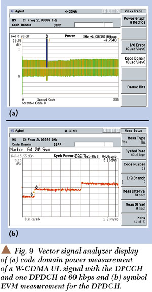
Figure 10 shows the de-spread symbol power in combination with the chip power for a UL signal. Analyzing the symbol power for a channel in combination with the chip power versus time is particularly useful for system integrators to analyze the power amplifier response (ripple) to a power control command.

DEMODULATED BITS
As shown in Table 1, the UL DPCCH can have different slot structures. The DPCCH may consist of the pilot, transmit power control (TPC), transport format control indicator (TFCI) and feedback information (FBI) fields. Figure 11 shows a slot structure example for an UL DPDCH and DPCCH.


By obtaining the demodulated bits after HPSK de-scrambling and de-spreading for each code channel, the correct bit patterns can be verified. It is particularly important to verify the bits for the different DPCCH fields, as shown in Figure 12. For example, the TPC bits should be verified, since power control is critical to system performance.

The demodulated bits measurement is an important troubleshooting tool for baseband engineers to identify coding, interleaving and power control bit errors. In many cases, it can help clarify situations where the BTS and the UE are having problems communicating with each other. Analyzing the demodulated bits may confirm whether the error is coming from the UE coding and interleaving, or from the BTS de-interleaving and de-coding process.
CONCLUSION
W-CDMA supports both voice and high data rate applications. The UE can transmit several code channels to achieve high data rates in the UL. Code domain analysis of the W-CDMA UL signal can help system integrators, baseband engineers and RF engineers determine the health of the UE transmitter and identify many impairments throughout its development. *
References
1. 3rd Generation Partnership Project, Technical Specification Group Radio Access Network, Physical Layer -- Spreading and Modulation (FDD), Release 99, 3G TS 25.213 (v3.3.0).
2. HPSK Spreading for 3G, Agilent Application Note 1335, Literature Number 5968-8438E.
3. Designing and Testing 3GPP W-CDMA User Equipment (UE), Agilent Application Note 1356, Literature Number 5980-1238E.
4. Testing and Troubleshooting Digital RF Communications Transmitter Designs, Agilent Application Note 1313, Literature Number 5968-3578E.
5. 3rd Generation Partnership Project, Technical Specification Group Terminal -- Terminal Conformance Specification, Radio Transmission and Reception (FDD), Release 99, 3G TS 34.121 (v3.1.0).
 Marta Iglesias-Xamani holds a BSEE from the Universitat Politecnica de Catalunya in Spain. During her career she has performed technical support for RF and microwave spectrum analyzers. Currently she is a wireless industry marketing engineer for Agilent Technologies, where she is responsible for understanding the test needs of the wireless communications industry.