
Editor’s Note: With the increasing number of cellular bands for 4G/LTE, the mobile RF front-end’s critical component has shifted from the power amplifier to the filter. Surface acoustic wave (SAW), and, more recently, bulk acoustic wave (BAW) filter technology has been addressing the challenges in the mobile RF front-end that currently uses 40+ filters (and growing). This market growth has attracted new market entrants so Microwave Journal compiled information from three such companies—Akoustis, OnScale and Resonant—offering new solutions for the SAW/BAW market.
XBAW RF Filter Blazing Into Higher Frequency Spectrum
Dave Aichele
Akoustis Technologies
Huntersville, N.C.
BAW RF filters are high performance semiconductor components primarily used in mobile smart phones. They address the stringent size requirement for high levels of integration and provide superior performance compared to SAW and ceramic filters, therefore improving the battery life and reducing the number of dropped calls to end users. These high performance components offer low insertion loss and high selectivity required to meet the demanding coexistence requirement for difficult FDD and high frequency TDD 4G/LTE and emerging 5G bands. Current multimode, multiband mid- to high-tier smartphones utilize > 50 filters and experts foresee that including 5G bands will push that number to > 70 filters.
Solidly mounted resonator (SMR) and film bulk acoustic resonator (FBAR) are the two dominant BAW resonator technologies currently utilized in BAW RF filters due to their high Q-factor, high operating frequency and good power handling. The BAW RF filter market is currently served by a duopoly that has historically supplied > 95 percent of the market, where both company’s core material technology is based on a sputtered poly-crystalline piezo-electric aluminum nitride (AlN) deposited by physical vapor deposition (PVD) techniques.
Single Crystal RF BAW Filter Technology
Akoustis Technologies is an emerging new entrant in the projected $5.8 billion BAW filter market dominated by mobile RF filters.1 Leveraging a patented BAW resonator process (called XBAW) combined with an integrated design and manufacturing (IDM) business model, Akoustis is blazing new territory and focused on becoming the first commercial supplier of BAW RF filters for applications above 3 GHz.
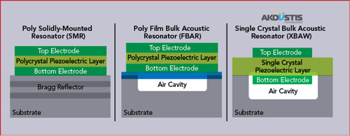
Figure 1 Cross section images of BAW resonators.
Akoustis has introduced a new approach of utilizing high purity, single crystal piezo-electric AlN material in BAW RF filters (see Figure 1). Epitaxially grown, metal-organic chemical vapor phase deposition (MOCVD) single crystal AlN has inherently higher crystal quality compared to PVD poly-crystal AlN. This improved crystal quality has shown improvements in acoustic velocity and piezo-electric mechanical coupling coefficients. In addition, the thermal conductivity of single crystal AlN is 2× higher than poly-crystal AlN that degrades as film thickness decreases, which may result in a constraint on power capability for traditional FBAR resonators, especially at higher frequencies. In all BAW technologies shown in Figure 1, the resonance frequency is determined by the thickness of the material stack and the effective propagation velocity of the acoustic wave. A higher propagation velocity in the AlN piezo-material results in higher operating frequencies for the same thickness. These three factors; improved acoustic velocity, improved piezo-electric coefficients and improved thermal conductivity enable XBAW RF filters constructed from single crystal, epitaxially grown MOCVD-AlN piezo-electric materials to offer better performance (power handling, insertion loss, bandwidth and skirt steepness) than PVD-AlN based BAW RF filters, especially for high frequency and high-power applications (see Figure 2).
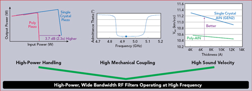
Figure 2 Three performance features of single crystal piezo-electric material.
In June 2017, Akoustis completed the strategic acquisition of a MEMS fab located in Canandaigua, N.Y. With this acquisition and subsequent consolidation of all its manufacturing processes, Akoustis now has an internal, ISO-9001 certified 122,000 sq. ft. commercial wafer-manufacturing capability which includes class 100/1000 cleanroom facility, tooled for 150 mm diameter wafers and an operations team to conduct research, development and production of its XBAW RF Filters. In addition, Akoustis is in the process of transitioning DoD Trusted Foundry accreditation for MEMs wafer processing, packaging and assembly, enabling Akoustis to be a supplier for DoD programs requiring specialized filters and Trusted Foundry certification.
RF BAW Filter Markets
Akoustis is the only pure play BAW RF filter company targeting the mobile high band 4G/LTE and emerging 5G applications. This market is by far the largest and made up of filter competitors engaging mobile phone OEMs and ODMs, RF front-end (RFFE) module manufacturers (some with captive BAW filter technology) and transceiver manufacturers. The push to higher frequency and the wide bandwidth requirement necessary to support the enhanced Mobile Broadband (eMBB) feature of 5G will tax existing SAW and poly-crystal BAW filter technology. Single crystal RF BAW technology will enable the development of higher performance, wider bandwidth BAW RF filters for 5G n41, n77, n78 and n79 bands (or sub bands) operating in 2.6 to 5 GHz spectrum with bandwidths that range from 200 to 900 MHz.
Beyond mobile, there are two additional markets that will be well served with access to single crystal RF BAW technology. Advanced Wi-Fi CPE architectures including 802.11ac multi-user MIMO (MU-MIMO) are experiencing faster uptake, driving the demand for smaller components as the complexity within Wi-Fi infrastructure devices is increasing. This trend is expected to continue, especially as 802.11ax is finalized and implemented in next generation tri-band routers that operate at 2.4, 5.2 and 5.6 GHz, simultaneously. Ultra-small passband 5.2 GHz BAW RF filters provide low 1.2 dB typical insertion loss over 160 MHz covering U-NII-1 and U-NII-2A bands with typical 52 dB attenuation across 345 MHz to meet the stringent rejection requirements enabling coexistence with U-NII-2C and U-NII-3 bands (see Figure 3). Incumbent Dielectric Resonator (DR) filters are 23× larger and require shield cans to mitigate interference issues degrading isolation performance.
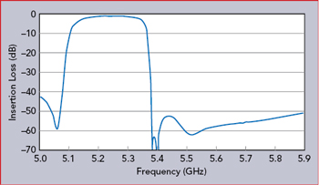
Figure 3 5.2 GHz BAW RF filter with typical 1.2 IL and > 50 dB attenuation.
The infrastructure market is looking at full dimension-MIMO or Massive MIMO architectures which use large antenna array each with its own transceiver configuration to offer much higher spectral efficiency. These new basestation systems will probably be the primary solution for emerging 5G and an alternative to traditional macro-cell BTS for 4.5G and 4.9G LTE networks. FD-MIMO architectures support both FDD and TDD bands and offer 1 to 4 W average powers in 32T32R to 64T64R configurations operating in the 2 to 5 GHz spectrum. These large array systems will need an alternative filter technology to enable size/weight reduction and high volume, surface mount assembly. Traditionally macro-cell style cavity filters are large in size and typically require manual assembly so are not ideal for FD-MIMO systems. Poly-crystal BAW RF filters are used in pico- and micro-cell BTS but may fall short on power handling above 1 W. High-power single crystal technology offers a potential paradigm shift to the major BTS OEMs developing 5G FD-MIMO systems. Akoustis has demonstrated BAW RF filter die mounted on standard laminate capable of handling > 10 W average power at 2.6 GHz (see Figure 4). This power handling provides plenty of power margin headroom for the design of RF BAW filters that offer smaller form factor, surface mount assembly at semiconductor price levels.
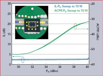
Figure 4 2.6 GHz BAW RF filter—WCDMA adjacent channel power ratio results.
Summary
Akoustis Technologies is a new entrant to the multi-billion RF filter market and blazing its own path through material science innovation in single crystal piezo-electric enabling high performance BAW RF filters in the 3 to 6 GHz spectrum for emerging 5G mobile, Wi-Fi and infrastructure applications. Beyond these largest markets, Akoustis is eyeing additional markets such as automotive C-V2X (or DSRC) and military IF/RF filters for L-, S-, C- and X-Band phase radar and communication systems.
Enabling Design of Next-Generation RF Filters for 5G
Gerry Harvey
OnScale
Cupertino, Calif.
While 4G LTE and LTE-Advanced technologies are still being deployed worldwide, the next generation in wireless communication promises a paradigm shift in throughput, latency and scalability. By 2025, the emerging wireless 5G market is expected to reach a total value of $250 billion.2 SAW filters and BAW filters are already used in 4G devices and will compete for the emerging 5G market. Adoption of 5G will see a significant increase in the number of filters required in a handset, with 4G models already employing 40+ filters. This puts the onus on 5G manufacturers to rapidly innovate new filter designs to capture a share of the growing market. Such innovations tend to offer a “winner take all” prospect such as the FBAR filter ushering in an entirely new product that captured a large percentage of the 4G/LTE market segment.
SAW/BAW Design
To help drive this new level of innovation, OnScale has developed a cloud-enabled simulation platform optimized for Multiphysics analysis of piezoelectric devices such as SAWs and BAWs. This approach is being used to reduce cost, risk and time to market for these products.

Figure 5 Full-3D model of a SAW filter in resonance.
Optimization of SAW/BAW filters is a challenging task due to the complexity and size of the devices. OnScale is well-suited for these kinds of problems, taking a highly efficient Finite Element Analysis (FEA) approach and seamlessly deploying this on the cloud. Figure 5 shows a SAW filter with 100 interdigitated pairs and 20 grating fingers modeled in full 3D. The zoomed-in portion shows the simulated surface velocity at a given time-step. The entire model can be run in a matter of hours which is a feat even the most powerful legacy solvers on the market are typically incapable of doing.
Optimization of this design is achieved using the cloud, where hundreds of these models can be simulated simultaneously to allow exploration of a design space defined by the variation of specific parameters. One of these iterations reveals a sweet spot where Q is maximized and spurs are minimized in the impedance of the device. Figure 6 shows the chosen design’s impedance versus frequency in this example.
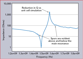
Figure 6 Impedance plot of an optimized SAW design in full-3D.
FBAR Design Example
FBAR filters, unlike their surface and bulk silicon counterparts, use piezoelectric thin films over cavities with resonant frequencies between 100 MHz and 10 GHz. A range of different shapes and sizes can be used depending on the performance requirements, with early designs using square shapes and more advanced designs using pentagons. Figure 7a shows a layout of a pentagonal FBAR resonator that has been imported into OnScale from a GDSII file. An image of the instantaneous surface velocity from the simulation is shown in Figure 7b.
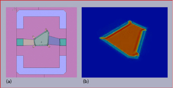
Figure 7 GDSII import and simulation of a pentagonal FBAR filter.
A major challenge for designers is ensuring that filters do not support strong lateral resonances that corrupt passband performance. Resonators with non-parallel sides, such as those shown in Figure 8, support weaker lateral resonances than ones with parallel sides. However, optimizing these shapes empirically is expensive and time consuming. Ideally, an engineer would use full 3D simulation for this optimization process, but this is considered impractical due to the extremely large computational requirements and time demanded by legacy FEM tools. The cloud method solves this problem, delivering rapid insights into these complex electro-mechanical systems and opens entirely new solution spaces for engineers to explore.
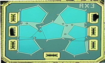
Figure 8 Die photo of an FBAR employing multiple pentagonal resonators.3
To demonstrate this capability, a 3D model of a pentagonal FBAR was constructed and a generic algorithm was used to optimize the design of the filter to minimize lateral resonances. Genetic algorithms mimic the process of natural selection to guide successive populations of candidate designs towards a global optimum. Each population of designs was simulated in parallel on the cloud, as shown in Figure 9.
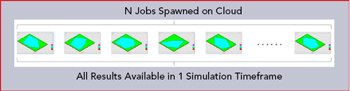
Figure 9 Parallel design study on the cloud.
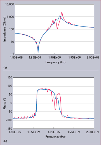
Figure 10 Comparison of simple square design (red) and optimized pentagonal design (blue).
The model was run for 52 generations and a total of 3,640 designs were investigated. It ran for a total of 68 hours and utilized 8.67 GB of memory. The simulation tool was connected to MATLAB’s Global Optimization Toolbox, which allowed various parameters to be tracked during the run including the current best design. The optimal designs were found to have edges angled relative to the substrate edges to avoid strong reflections, whereas the worst design had three edges close to parallel with the substrate causing increased lateral mode activity.