
Extending Gold Thick-film Technology through Materials and Process Development
Meg Tredinnick and David Malanga
Heraeus Inc., Circuit Materials Division
West Conshohocken, PA
New powder and screen technologies have allowed for the development of a thick-film gold paste that meets a difficult list of requirements. This new Au and Al wire bondable conductor is able to print thin, cost-effective, fine line patterns (down to 3 mils) while meeting a wide variety of physical and electrical requirements. Data are presented to show the wide range of wire types, both Au and Al, that can be used on the gold conductor, with reliable results. Additional data are presented to demonstrate the material's excellent back-lit density and low resistivity, as well as its compatibility with a variety of solderable conductors to allow for its use in mixed metallurgy circuits. These properties were achieved at a fired film thickness of 5 to 8 µm, which provides for significant cost savings for the circuit manufacturer.
There are many demands placed on thick-film conductor materials. The advent of lightweight, hand-held electronics requires high conductivity and fine-line geometry. Increased chip functionality requires additional input/outputs, which demand more reliable and versatile wire bonding. Thick-film gold materials are ideally suited for this type of demanding application. The high conductivity and wire bond characteristics of thick-film gold pastes meet many of these requirements. As circuits get smaller and more complex, the thick-film gold properties become more critical. Increased wire bond versatility coupled with finer geometries and high conductivity is a must to meet these new demands.
Along with more demanding applications comes a need for reduced manufacturing costs. Lower costs can be achieved by reducing material usage and easing processing. A robust thick-film gold material that lends itself to high speed, automatic wire bonding allows for less operator involvement and reduced manufacturing time. By increasing the coverage of the thick-film gold paste, the circuit manufacturer can gain significant cost savings. This article describes a thick-film gold material that meets these demands and, when processed appropriately, offers fine line geometries.
Au POWDER EVOLUTION
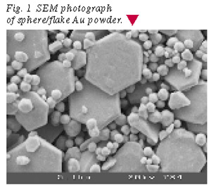
The traditional type of gold (Au) powder that was used in gold conductor thick-film pastes in the 1980s was the sphere/flake powder. The main advantages of this powder were that there was a low amount of agglomeration and the fired structure had a low tendency to blister. However, due to the more open structure of the fired film, wire bonding could produce sporadic results. Figure 1 shows a scanning electron microscope (SEM) photograph of this type of powder.
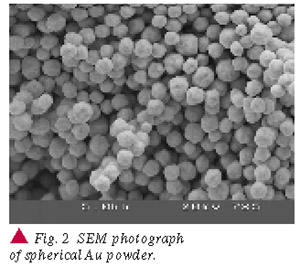
The next generation of powder was a spherical powder. Dense fired films were achieved from the monosized particles. However, blisters could occur if the structure was not processed properly. Figure 2 shows a SEM photograph of the spherical powder.
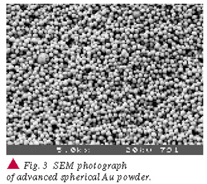
A SEM photograph of the newest technology is shown in Figure 3 . The advanced spherical gold technology provides for agglomerate-free powder because of the use of advanced dispersion techniques. This type of powder provides extremely dense fired films that demonstrate excellent wire bonding performance.
WHY IS ALUMINUM WIRE BONDING REQUIRED?
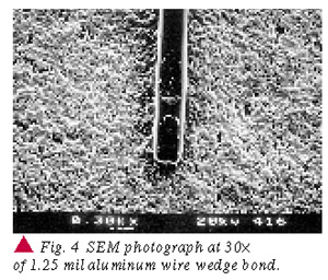
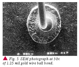
The main reason for using aluminum (Al) wire for bonding is that ultrasonic wire bonding can be utilized. Even though Au wire can be used for ultrasonic bonding, aluminum is the preferred wire.1 The advantage of ultrasonic bonding is that it requires no heating of the substrate or the die that is being bonded. Another reason that aluminum wire is preferred is that bonding can be accomplished on finer pitch pads for aluminum wedge bonds than for gold ball bonds. The squash that is formed from a gold ball bond requires more space than the wedge formed on an aluminum wire. In both examples, 1.25 mil (31.25 µm) wire is used. Figure 4 shows the wedge bond of an aluminum wire where the width of the bond is 1.16 mils (29 µm), approximately the same size as the wire. Figure 5 shows the deformation from a gold ball bond with the same size wire. The diameter of the deformation is 6.48 mils (162 µm).
ALUMINUM WIRE BONDING CHALLENGES
When the advanced spherical Au powder was first used to produce a thick-film paste, the metal composition contained only gold. Therefore, only Au wire could be used for wire bonding. However, the need was present for a gold paste that could be bonded with aluminum wires.
The challenge when aluminum wire is used on a gold conductor is that Al/Au intermetallics form and Kirkendall voiding occurs. Kirkendall voids form when either the aluminum or the gold diffuses out of one region faster than it can diffuse in from the other side of the region. Valences pile up and condense to form voids.2 Figure 6 shows a heel imprint left on the fired film of an undoped gold conductor.
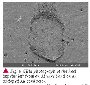
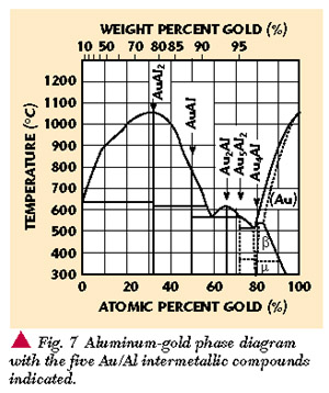
The beads seen along the bottom of the heel print indicate the Au/Al intermetallic formation. This condition occurred after aging the bond at an elevated temperature. Kirkendall voiding is also referred to as purple plague because the AuAl2 state of the intermetallic area is purple-colored. Al and Au in other states are different colors, such as tan or white. Figure 7 shows a phase diagram of gold and aluminum, with the five Au/Al intermetallic compounds indicated.2
These voids lead to premature failure of the bond between the aluminum wire and the Au conductor. Unfortunately, the intermetallic formation cannot be avoided. The challenge was to find a dopant to add to the gold paste formulation that would slow down the diffusion process and improve the adhesion of the aluminum wire.
EXPERIMENT
Literature confirms that dopants can be added to gold thick-film compositions to slow down the Au or Al diffusion and lengthen the life of the aluminum wire bond.2 Different dopants were tested using an existing aluminum wire bondable gold conductor as the control. From the wire bonding results received, a final formulation was selected.
Project goals were then established for the doped gold conductor. The most important factor was that the conductor is required to be wire bondable with both fine and heavy aluminum wires. Fine line printability down to lines and spaces of 3 mils (75 µm) and a very dense fired film were also required. In addition, high conductivity, good cosmetics and compatibility with other solderable conductors were desired.
WIRE BOND RESULTS
All of the initial wire bond testing was done with manual wire bonders. Wire sizes of 1.25 mil (31.25 µm), 5 mil (125 µm), 8 mil (200 µm), 10 mil (250 µm) and 20 mil (500 µm) were tested. Wire bonds were placed on gold conductor films that were printed on alumina substrates and multilayer dielectric pastes. Aging studies were performed at 150°C for up to 1000 hours.
Figure 8 shows the 1.25 mil aluminum wire adhesion results with the average adhesion values at each time interval tested. The key to these data is that the values are well above 3.5 grams. This level is the minimum bond strength requirement for 1.25 mil aluminum wire according to Mil Standard 883E. In addition, the minimum adhesion values were above the 3.5 gram requirement (not shown in this graph). By 1000 hours, all failures were still wire breaks.
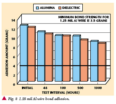
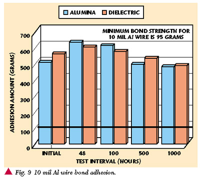
Figure 9 shows the 10 mil aluminum wire bond adhesion results. Again, the average and minimum adhesion results were well above the minimum requirement of 95 grams. Superior adhesion results were also obtained for the 5, 8 and 20 mil aluminum wires, plus the 1 mil gold wire and 1 * 5 mil gold ribbon that were tested. These data are not presented here, but are available upon request.
FINE LINE PRINTING CAPABILITY
The industry trends are for finer line resolution. However, manufacturers want to keep the cost of the circuit down by using screen printing techniques (vs. thin-film techniques such as etching). Currently, many thick-film circuit production facilities are successfully printing 5 mil (125 µm) lines and spaces, but the drive has been to go down to 3 mil (75 µm) on a consistent basis. This reduction is possible with the advanced new gold material by taking careful consideration of the process.
The five factors that affect print resolution are screen mesh, the amount of paste on the screen, squeegee speed, paste viscosity, printer setup and screen quality. The screen mesh is the most important factor. Print tests were performed with different mesh screens under the same screen printer conditions using traditional 325 and 400 stainless mesh screens.
In addition, a type 350SA screen was included in the test matrix. This type of screen is made from exceptionally strong and thin special alloy wires. With the increased strength of the wires, finer-sized wires can be used to achieve the same tension, increasing the open-area percentage of the screen. This increase in open area is significant because more open area minimizes the obstruction of the paste flow through the screen and increases the resolution capability of the pattern.3
For a 400 mesh stainless steel screen with 0.7-mil-diameter wire, there is 51 percent open area. For the 350SA mesh screen, with 0.63-mil-diameter wire, the percentage of open area increases to 61 percent. The switch to the 350SA screen made a noticeable difference in the ability to achieve 3 mil (75 µm) line resolution consistently. Figure 10 shows a SEM photograph of the 3 mil (75 µm) lines and spaces achieved with this type of screen.
With regard to the other factors that affect print quality, improved print resolution may be achieved by flooding the screen with paste using a flood bar, using print speeds greater than six inches per second, ensuring that the screen is not sagging or showing any other defects and using pseudoplastic paste rheology. Figure 11 shows a schematic of the screen printing process. It is desirable to keep the paste close to the tip of the squeegee. This technique will prevent paste from seeping through the pattern in the screen prematurely. When seepage occurs, the bottom of screen must be wiped more frequently to ensure the cleanest print definition. The correct pseudoplasticity of the thick-film paste will prevent seepage from occurring.
FIRED FILM DENSITY
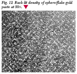
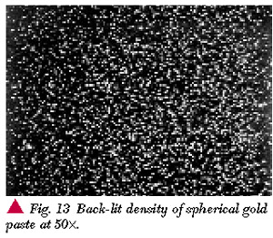
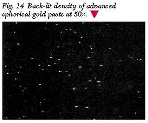
To examine the back-lit density of the fired surface, parts were viewed under magnification at 50*, with a light source under the part. Figures 12, 13 and 14 show photographs of the back-lit density for the sphere/flake gold conductor, the spherical gold conductor and the advanced spherical gold conductor, respectively. The extremely dense fired surface is apparent with the advanced spherical gold conductor surface. The key is that the other two conductors were printed at a fired film thickness of 10 to 12 µm, whereas the advanced spherical gold conductor was printed at a fired film thickness of 5 to 8 µm.
RESISTIVITY
As part of the study, resistivity measurements were conducted on 25-mil-wide lines vs. 10-mil-wide lines to compensate for the natural bias of a screen printed line. On a printed line, some curvature will occur; it will not be an exact square. This natural bias will decrease the number of squares in the pattern. Using a 25-mil-wide line reduces the effect of the natural bias. With less effect on the total number of squares, a more accurate resistivity measurement may be achieved.
The resistivity of this advanced new gold conductor is 3.6 mO/sq. at 10 µm fired film thickness. This result is outstanding for a doped gold conductor because, when a dopant is added to a pure gold conductor, resistivity increases. Furthermore, this increase seen in the doped gold conductor is not significant when compared to the resistivity of a pure gold conductor.
SURFACE APPEARANCE
The new gold conductor displayed a shiny fired surface appearance. The cause of this shine is due to a large grain size. A Tencor profilometer was used to test the surface roughness. A paste made with the sphere/flake powder had a surface roughness that was two times the surface roughness of a paste made with the advanced spherical powder. A smooth surface is desired because it facilitates more consistent wire bonding.
COMPATIBILITY WITH SOLDERABLE CONDUCTORS
As a further cost savings, it is desirable to use silver and silver/palladium conductors in conjunction with gold conductors. Silver-based conductors are frequently used on the inner layers of the circuit to reduce costs. Applications may also require solderable pads on top of the circuit, where components need to be attached. A variety of different conductors were tested with the advanced spherical gold paste as the top and bottom conductors. The results revealed that the order of application matters. The same results were not obtained for certain solderable conductors when the gold paste was switched from top to bottom. Incompatibility occurred in certain combinations due to the mobility and sintering dynamics of the frits in each paste.
Some of the solderable conductors contained a high amount of Bi and, when this type of conductor was used under the gold conductor, the frits became trapped and caused blistering. However, when the paste containing a high amount of Bi was used on top of the gold conductor, no blistering occurred. Since most of the standard solderable conductors have been tested with the advanced spherical gold conductor, the manufacturer can recommend which solderable conductors to use based on the user's circuit design.
FIRED FILM THICKNESS
As mentioned previously, the use of 325 to 400 mesh screens achieved a fired film thickness of 5 to 8 µm for the spherical gold conductor paste. This result is due primarily to the tighter packing density achieved from the spherical powder size. All the testing in the study was done on fired films in this thickness range; therefore, the thinner print does not appear to affect performance.
The main benefit is that the thinner print thickness allows for better coverage and, ultimately, cost savings. Coverage for the advanced spherical gold conductor was calculated to be 118 cm2 /gram vs. the older sphere/flake conductor, with coverage of 89 cm2 /gram. A 32 percent increase in coverage is a direct cost savings to the circuit manufacturer.
CONCLUSION
A combination of new gold powder technology and advanced manufacturing techniques makes it possible to achieve fine line resolutions of 3 mils (75 µm) through screen printing methods. The capability to perform finer line screen printing results in smaller, denser circuitry. It has also been shown that the advanced gold conductor paste produces a versatile, dense fired film that has exceptional wire bonding performance with a wide range of aluminum wire sizes.
ACKNOWLEDGMENT
A version of this paper was presented at the IMAPS 2000 Technical Conference. It was reprinted with permission from the Proceedings of the International Symposium on Microelectronics , September 1822, 2000, Boston, MA. For more information, contact Meg Tredinnick (meg@4hcd.com) or David Malanga (dmalanga@4hcd.com) at Heraeus Inc., Circuit Materials Division, 24 Union Hill Road, West Conshohocken, PA 19428, (610) 825-6050, fax (610) 825-7061 or Web site: www.4cmd.com. *
References
1. Roydn D. Jones, Hybrid Circuit Design and Manufacture , Chapter 8, Marcel Dekker Inc., 1982, pp. 109.
2. George Harman, Wire Bonding in Microelectronics: Materials, Process, Reliability and Yields , Second Edition, Chapter 5, McGraw-Hill Publishers, New York, 1997, pp. 116127 and 128130.
3. Microcircuit Engineering Web Site -- www.microcircuit.com.