

It is well known that three-dimensional electromagnetic (3D EM) solvers have had a tremendous effect on how passive microwave circuits are designed today. In the not-so-distant past, a typical microwave filter design cycle would start with modeling on a circuit simulator, followed by prototype manufacturing and measurement. Often, the coarse design phase did not lead to compliant prototypes, and the prototype had to be “redesigned,” taking days or weeks with copper tape and modifications in the machine shop. Several such cycles were frequently needed before the prototype met requirements.
Today, the initial design phase is probably little changed, but we now build and modify the prototypes in 3D EM solvers instead of making measurements on machined models. A physical prototype fulfilling all requirements is most often achieved in just one pass, which underscores the impact of EM solvers on development time and cost.
With EM solvers, today’s microwave engineer can develop much more complex, innovative and integrated solutions than before. “Wild” ideas can be tested and included in designs if they pass. Yet, even today, the direct analysis and optimization of complex mechanical filters in 3D EM solvers is often too resource intensive and time-consuming to be usable in practice. An often-used alternative is to combine 3D EM solvers with circuit modeling techniques.1
CO-SIMULATION
Most often, a filter project is initiated by synthesis and simulation in a circuit simulator or comparable tool. In this work, a filter and coupling matrix synthesis (CMS)2 tool is used for this. The output is a coupling matrix that describes all the necessary couplings in the filter. The principal task of the work following synthesis is to convert the coupling matrix into a physical filter.3 It is here that 3D EM simulators find their use. The main concern is couplings. The most common way to verify couplings in a manufactured prototype filter is to tune in all resonators until a “nice” filter characteristic is obtained. If bandwidth, stopband notches and return loss are as expected, the couplings are fine; if not, they need to be modified.
When a 3D EM simulator is used instead of a machined prototype, tuning of the resonators in the 3D EM model is still necessary to verify the couplings. Very often, resonator tuning is realized with tuning screws whose actual positions are not necessary to know in detail. The 3D EM simulator must, however, finish optimizing these screw positions to arrive at a usable filter characteristic. Since a change of only a few hundredths of a millimeter can greatly affect a filter characteristic, the EM simulator can waste a lot of computing time on this task. Even for moderately complex filters, the task of performing a full-wave optimization, which includes resonator tuning, may well be too time-consuming to be feasible. It is for this reason that co-simulation is used.
This is demonstrated by Swanson and Wenzel for a 5-pole combline filter.1 Internal lumped ports are placed at the end of each resonator in the 3D EM model, and the resulting 7-port S-matrix is exported to a circuit simulator, where lumped capacitors are connected to the internal ports. In the circuit simulator, these tuning capacitances are quickly optimized to reveal the filter characteristic, and hence the couplings. Co-simulation may also be implemented in other ways.4-5 In this work, the method described by Swanson and Wenzel is used to analyze and design an extremely broadband, multipole, coaxial cavity filter with multiple cross couplings.

FILTER DESIGN
The filter, intended for a cable TV distribution system, has the specifications shown in Table 1. With greater than 70 percent relative bandwidth and an extremely sharp cutoff, this filter type is sometimes referred to as a “brick wall” filter. The steep transition between the lower stopband and passband calls for resonators with high unloaded Q. It is at the edge of the passband—at the “shoulders”—that the filter performance mainly benefits from high-Q resonators. The temperature range makes it necessary to include some bandwidth allowance for temperature drift. The actual value depends on factors such as filter type, materials and resonator layout. A starting point could be 0.5 MHz, since the operating temperature range is quite limited. This means that the original 12 MHz transition band is reduced to 11 MHz. The power level is low enough that no special precautions are needed to avoid breakdown.
Accurate synthesis of strongly asymmetric, ultra-wideband filters is no easy task. As mentioned previously, CMS is used in this work, which yields results similar to lumped-circuit models but is only accurate for bandwidths up to approximately 10 percent. The greater than 70 percent relative bandwidth requirement is far beyond the range where CMS can be expected to provide reliable results for coupling values and resonant frequencies. The CMS synthesized filter is, however, a suitable starting point for an HFSS model,6 the 3D EM solver used throughout this article. The shortcomings of CMS are overcome when the HFSS model is optimized in the ADS7 circuit simulator.

Figure 1 CMS synthesized filter characteristic.
A CMS synthesized, tenth-order bandpass filter to fulfill the specifications is shown in Figure 1. Filter synthesis in CMS is not addressed here, but design information is available.2 Given the order of the filter and the available space, it is realized as a coaxial cavity combline design. The four transmission zeroes are achieved with four triplets in series, positioned at 552, 548, 535 and 500 MHz, respectively. Triplets in series are much more robust than other more “advanced” topologies—for example, a folded topology—in terms of sensitivity to tolerances, tuning accuracy and temperature variation. Table 2 shows the corresponding coupling matrix synthesized in CMS. All values are in MHz and empty cells correspond to zero coupling. Only values on and above the main diagonal are shown, where the main diagonal contains the resonant frequencies of the individual resonators. The four couplings above the main line are non-adjacent couplings (cross or x-couplings). These x-couplings are negative and, therefore, capacitive. Resonator 1, for example, has a resonant frequency of 887.4 MHz.
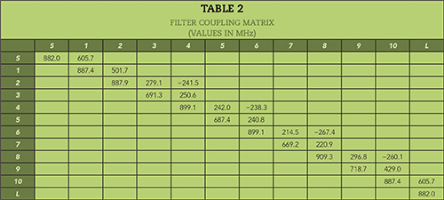
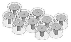
Figure 2 Layout of 10 resonator HFSS model.
Reviewing Table 2 yields several conclusions:
- Some of the resonators are detuned quite a lot compared to the center frequency of 882 MHz. The resonant frequencies span from 669 to 909 MHz, indicating that different resonator layouts should probably be used in the filter.
- The values just above the main diagonal are the main line coupling bandwidths. All couplings are positive (inductive) and have very high values. Combline resonators do not couple as strongly as, for example, interdigital resonators. Combline filters are therefore normally used for small to intermediate bandwidths. This limited coupling strength is addressed later in this article.
3D EM MODELING
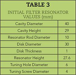
The first step in building the 3D model is to design a resonator that can be tuned over the desired range, has the right unloaded Q and does not violate any mechanical constraints. Dividing the available volume (190 mm x 115 mm x 45 mm) between 10 circular cavities and subtracting space for the walls, lids and headroom for tuning screws results in the filter layout shown in Figure 2. The individual resonators have the dimensions shown in Table 3.
The resonators are analyzed with the eigenmode solver in HFSS. The unloaded Q is approximately 2000 for aluminum. The layout can support the resonant frequencies in Table 2 below approximately 600 MHz. Three or more different layouts with smaller top disks are required for the resonators with resonant frequencies above 600 MHz. The first 3D model, however, uses the resonator design of Table 3 as a starting point.
The layout in Figure 2 has 75 Ω coaxial inputs at resonators 1 and 10. Due to the required strong couplings between the resonators, apertures are added in the sidewalls at the top of the cavities to allow lumped coupling between them. Simulation on two-pole boxes3 revealed that the strong couplings cannot be achieved just by placing the resonators in close proximity. The couplings must be implemented in a more direct way: for example, by loops or wires tapped to the top of the resonators. A schematic overview of the topology is shown in Figure 3.
In the HFSS model, lumped ports are placed at these tap points so that lumped components (inductors and capacitors) can later be inserted in the circuit model. Therefore, the coupling loops are not included in the HFSS model; they are added later in the circuit simulator.
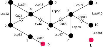
Figure 3 Filter topology corresponding to Figure 2.
Figure 4 shows the port details in resonator 1; the ports are marked in red. The port at the coaxial input is a wave port; all other ports are lumped ports. One lumped port is implemented as a circular disk at the end of the tuning screw. One of the rectangles is a lumped port defined between the upper surface of the resonator disk and the lid (ground). The other rectangular lumped port is defined between the tip of the inner conductor of the coaxial line and the lid. Between these two ports, an inductor is later connected in the circuit simulator. Common for all ports, they are defined between a point in the filter and a reference point, which is usually ground.
Lumped ports are placed on appropriate points in all resonators. Resonators 4 and 8, for example, both have four lumped ports placed along the top disk perimeter to account for two x-couplings and two mainline couplings on each resonator. For a complex filter such as this, a large number of ports are required. One for each tuning screw, two for each coupling, plus two input/output (I/O) waveguide ports equals 42 ports total.
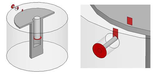
Figure 4 Assignment of ports (red faces) in Resonator 1.
With the HFSS model complete, a frequency sweep obtains the 42-port S-matrix for circuit simulation. In the initial design phase, the filter is considered lossless.