
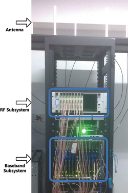
Figure 1 Hardware platform.
This article describes a broadband 8×8 MIMO RF subsystem with large area coverage for next generation wireless local area networks (WLAN) in the 5 GHz band. Measurements demonstrate the capability to operate over a long range of 80 m at a high data rate of 1 Gbps, due to its 23 dBm transmitter, -70 dBm sensitivity, 50 dB dynamic range receiver and 8 dBi high gain antenna. The EVM of transmitter and receiver are 2.6 and 3.2 percent, respectively, for an 80 MHz 64 QAM signal. The 8×8 RF subsystem has been successfully integrated into an IEEE 802.11ac prototype system. Because broadband OFDM signals employed in 802.11ac WLAN standards are more sensitive to non-ideal RF system characteristics such as phase noise, I/Q imbalance and interference, their effects are analyzed and mitigations are incorporated. Design details, fabrication considerations and measurement results are presented.
Increasing demand on high data rate, long range wireless communication networks has driven the advancement of wireless local area network (WLAN) standards. In 1999, 802.11b dictated a maximum data rate of 11 Mbps at 2.4 GHz, increasing to 54 Mbps at 5 GHz with 802.11a and at 2.4 GHz with 802.11g in 2003.1 In 2009, 600 Mbps was achieved in 802.11n by using additional multiple-input-multiple-output (MIMO) antennas. With the continuing development of laptops and smartphones, however, there is a need for even larger amounts of data sharing,2 driving the creation of a new standard for higher data rate WLAN. The new 802.11ac standard, also known as very high throughput (VHT), is capable of a 500 Mbps data rate with one spatial stream in the 5 GHz band and greater than 1 Gbps with multiple spatial streams. It benefits from new features, such as wider channel bandwidth, a higher-order modulation scheme and more spatial streams.
There are three challenges in the design of an RF subsystem for future WLAN.3 First is the transceiver’s higher sensitivity to I/Q imbalance and channel gain flatness due to its wide channel bandwidth. Second is a higher sensitivity to carrier frequency offset and phase noise than single carrier systems.4 Third is a higher peak-to-average ratio (PAR) caused by the complex modulation scheme, which requires more power back-off in the power amplifiers (PA).
Several methods are employed in this system to address these challenges and achieve excellent RF performance. Sufficient noise decoupling of the reference signal generation module and phase-locked loop (PLL) module improves the phase noise performance of the RF subsystem. The use of a broadband modulator and extra operational amplifiers ensures good I/Q balance within the 80 MHz bandwidth. Close attention to the printed circuit board (PCB) layout and metallic shields between modules reduces interference.
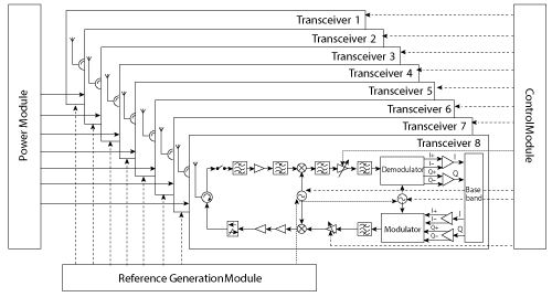
Figure 2 RF subsystem block diagram.
The measured communication range is as much as 80 m with a 1 Gbps data rate. Transmitter output power is as high as 23 dBm, which provides enough margin for the PA power back-off needed by the complex modulation scheme. The receiver operates over a large dynamic range of more than 50 dB. A parallel-fed twin-dipole array is used to form the 8 dBi high-gain antenna. The measured EVM of the transmitter and receiver using an 80 MHz 64 QAM signal is 2.6 and 3.2 percent, respectively.
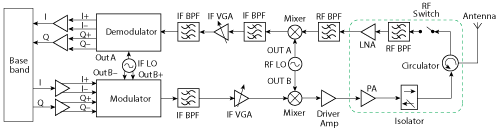
Figure 3 5.8 GHz WLAN RF transceiver block diagram.
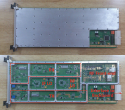
Figure 4 5.8 GHz WLAN RF transceiver prototype.
SYSTEM OVERVIEW
The network is composed of one access point (AP) and user equipment (UE), which can be distributed throughout a building. The hardware platforms are the same at all the nodes (see Figure 1). The RF subsystem block diagram is shown in Figure 2. It has an operating frequency range of 5.76 to 5.84 GHz for an 80 MHz channel bandwidth and consists of one power module, one control module, one reference signal generation module and eight RF transceiver modules. The power module converts 48 to 6 VDC with a DC to DC converter. The control module guarantees communication between the baseband circuitry and RF transceivers. The reference signal generation module, which consists of a 10 MHz oven controlled crystal oscillator (OCXO) and a PLL, provides a 10 MHz reference signal to each of the eight transceivers.
It works in a time-division-duplex (TDD) mode. The transceiver has an RF port to the antenna and an I/Q interface to the baseband. The peak-to-peak voltage of I/Q signals between the RF subsystem and baseband circuitry is 500 mV. The transmitter and receiver share one antenna by using a circulator as shown in Figure 3. Each transceiver has its own antenna, so there are eight antennas in total.
MITIGATION OF NON-IDEAL SYSTEM CHARACTERISTICS
Phase Noise
Improper setting of phase-locked loops (especially the loop filter bandwidth), a noisy power supply and reference frequency jitter are the main sources of phase noise. In the TDD mode, amplifiers on Tx and Rx paths are switched on and off with each communication burst in order to minimize power consumption. Power consumption changes dramatically between Rx mode and Tx mode, introducing noise. Unless the noise is thoroughly decoupled, it can affect the crystal oscillator and cause jitter in the reference. Phase noise is reduced by properly setting the crystal oscillator loop filter bandwidth, using an ultra-low noise, low dropout, linear regulator in the PLL power supply and employing tantalum capacitors for further decoupling.
It is also important that the 10 MHz reference be distributed to each RF transceiver without introducing jitter, especially when multiple RF boards are inserted in the RF subsystem. This is accomplished with an ultra-low jitter LVCMOS fan-out buffer to distribute the reference to the eight RF transceivers.
I/Q Imbalance
Theoretically, a phase imbalance (θ) and an amplitude imbalance (β) degrade SNR according to5

If SNR degradation of less than 2 dB is required to achieve an SNR = 21 dB, the phase imbalance should be less than 5 degrees and the amplitude imbalance should be less than 0.5 dB.6 In practice, I/Q imbalance has a greater impact on wide bandwidth systems.
Asymmetry in the PCB layout and different trace lengths for the baseband I and Q signals contribute to I/Q imbalance. For a modulator or demodulator, impurities in the LO signal also contribute to I/Q imbalance. A bandpass filter placed between the PLL and the demodulator can help to filter out undesired harmonics, while amplitude imbalance is compensated by adjusting the feedback resistor of the operational amplifier and phase imbalance is compensated by placing shunt capacitors in I/Q signal paths.7
Interference
Shielding between different parts of the RF transceiver is critical, especially those parts with large power.8 Different functional blocks are separated by a metal frame as shown in Figure 4. The large LO signal and its harmonics can be coupled to the RF front end through the dielectric substrate or other paths. To address this, LC lumped filters in the output path of the LO signal filter out the relatively high LO harmonics. A high isolation mixer is also used to reduce LO leakage.
Carrier feedthrough is mainly caused by imbalances in the DC offset between I/Q signals at the input of the modulator. The operational amplifiers shown in Figure 3 act as buffers between the baseband signals and the modulator, and can also provide DC offset compensation for the I/Q signals. Tuning the DC offset of the I/Q paths can effectively suppress the carrier feedthrough to a level below -55 dBc.
RF TRANSCEIVER AND ANTENNA DESIGN
Structure
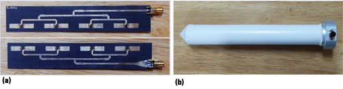
Figure 5 Antenna prototype (a) and its package (b).
The transceiver is integrated on a 1.5 mm thick, four-layer PCB.9 The first layer is on a Taconic TLX substrate, with εr =2.55, h=0.5 mm. The others are on FR-4. The RF front end, shown in the green dashed line box in Figure 3, uses a two-layer PCB (εr =2.55, h=0.5 mm) to provide a good ground connection and proper heat dissipation for the PA. The two PCBs are fixed on one metal base and interconnected with adjacent microstrip lines. The RF band is from 5.76 to 5.84 GHz, with a 4.2 GHz LO frequency and a 1.6 GHz IF.
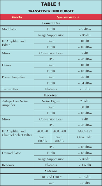
Link Budget
IEEE 802.11ac stipulates operation over 5 to 6 GHz with a 293 Mbps data rate (80 MHz bandwidth, 1 spatial stream, and 64 QAM 5/6) and a sensitivity of -58 dBm. The sensitivity for an 80 MHz QPSK signal is -71 dBm. The relation between sensitivity (Psen), thermal noise (Pnoise), noise figure (NF) and signal to noise ratio (SNR) can be expressed as

A noise figure of 7 dB (Pnoise = -95 dBm, SNR=17 dB for 80 MHz QPSK signal) is required to satisfy the -71 dBm condition. Gigabit-per-second data rates can be achieved by using multiple antennas and transceivers. The link budget of the transceiver is listed in Table 1.
Antenna
The high gain parallel-fed twin-dipole array antenna consists of four identical printed twin-dipoles with half wavelength separation. The two arms of the twin dipole are printed on each side of the substrate and connected by metal vias. This structure can also effectively suppress cross polarization. The feed network acts as a two-stage power divider. It is realized by parallel strips of the same width on each side of the substrate. When the feed lines are connected to different arms, the two dipoles have a 180 degree difference in phase, which means the dipoles work in the even mode.10 The antenna is fabricated on a 12.3 × 2.2 cm two-layer PCB, shown in Figure 5a, and is packaged in a plastic cylinder with a 3.5 mm SMA connector to the cable, shown in Figure 5b.
MEASUREMENT RESULTS
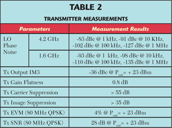
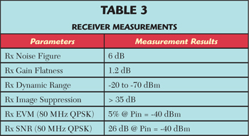
Performance is measured with a Keysight N8421A arbitrary waveform generator, R&S SMBV100A signal generator, Keysight N9020 spectrum analyzer and Keysight DSO91304A oscilloscope. Transmitter performance is summarized in Table 2, including phase noise of the local oscillator. Transmitter IMD3 and EVM performance is shown in Figure 6. Receiver performance is summarized in Table 3. Receiver EVM performance becomes worse with increasing bandwidth as shown in Figure 7. The receiver’s maximum input power is -20 dBm, and its minimum input power (sensitivity) is -70 dBm, resulting in a 50 dB dynamic range.
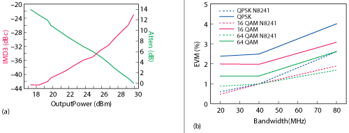
Figure 6 Transmitter measured results; IMD3 (a) EVM at 23 dBm output power (b).
The arbitrary waveform generator creates the baseband signal, which is upconverted to 5.8 GHz by the signal generator. The transceiver is tested using a 20 MHz LTE signal (which is also an OFDM signal) due to instrumentation bandwidth limitations. The measured transmitter and receiver EVM using the 20 MHz LTE signal is 2.1 and 2.2 percent, respectively (see Figure 8). Because of the lack of calibration for I/Q skew, EVM performance of the N8241A is poor (3.5, 2.4, and 2 percent for 80 MHz QPSK, 16 QAM, 64 QAM signal, respectively); therefore, the actual EVM might be better than the measured values. Measured versus simulated input return loss of the antenna and the radiation pattern at 5.8 GHz are shown in Figure 9. The antenna has the gain of 8 dBi at 5.8 GHz and a wide impedance bandwidth from 4.8 to 6.5 GHz. Figure 10 shows the operational system, where the cabinet on the left acts as a base station and the one on the right acts as the nearest mobile station. The data stream is transmitted and received through the antennas on the top of each cabinet.
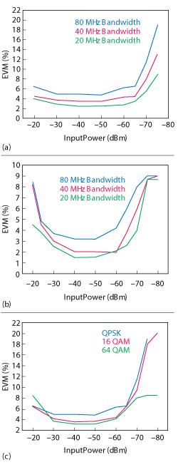
Figure 7 EVM performance of the receiver for QPSK signal (a) 64 QAM signal (b) 80 MHz signal (c).
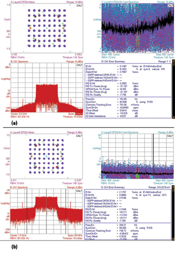
Figure 8 EVM measurement of the transmitter at 23 dBm output power (a) and the receiver (b) for 20 MHz LTE signal with 100 resource block.
CONCLUSION
An RF subsystem for future WLAN has been designed, fabricated and measured. The influences of phase noise, I/Q imbalance and interference are analyzed, and measures are taken to provide performance improvements. The RF receiver has low noise, wide dynamic range and high image rejection within the broad channel bandwidth. The RF transmitter has a high IMD3 and low EVM at 23 dBm output power. The antenna has 8 dBi gain at 5.8 GHz. The 8 × 8 RF subsystem has been used in an IEEE 802.11ac prototype system successfully with more than 1 Gbps throughput over an 80 m radius of coverage.
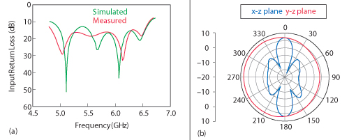
Figure 9 Antenna input return loss (a) and radiation pattern at 5.8 GHz (b).
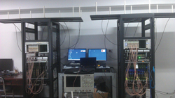
Figure 10 WLAN system operation scenario.
ACKNOWLEDGMENT
This work is supported in part by the National Natural Science Foundation of China under Grant 60702163, and in part by the National Science and Technology Major Project of China under Grant 2010ZX03007-002-01 and 2011ZX03004-003.
References
- G. Hiertz, D. Denteneer, L. Stibor, Y. Zang, X.P. Costa and B. Walke, “The IEEE 802.11 Universe,” IEEE Communications Magazine, Vol. 48, No. 1, January 2010, pp. 62-70.
- Rolf de Vegt, “802.11ac Usage Models Document,” IEEE, 802.11-09/0161r2, January 22, 2009.
- Greg Jue, “Tackling MIMO Design and Test Challenges for 802.11ac WLAN,” Microwave Journal, Vol. 55, No. 3, March 2012, pp. 88-96.
- T. Pollet, M. van Bladel and M. Moeneclaey, “BER Sensitivity of OFDM Systems to Carrier Frequency Offset and Wiener Phase Noise,” IEEE Transactions on Communications, Vol. 43, No. 234, February/March/April 1995, pp. 191-193.
- C.L. Liu, “Impacts of I/Q Imbalance on QPSK–OFDM–QAM Detection,” IEEE Transactions on Consumer Electronics, Vol. 44, No. 3, August 1998, pp. 984-989.
- L.H. Li, F.L. Lin and H.R. Chuang, “Complete RF-System Analysis of Direct Conversion Receiver (DCR) for 802.11a WLAN OFDM System,” IEEE Transactions on Vehicular Technology, Vol. 56, No. 4, July 2007.
- Z.Q. Yu, J.Y. Zhou, J.N. Zhao, T. Zhao and W. Hong, “Design of a Broadband MIMO RF Transmitter for Next-Generation Wireless Communication Systems,” Microwave Journal, Vol. 53, No. 11, November 2010, pp. 22-26.
- Z. Chen, W. Hong, J.Y. Zhou, J.X. Chen and C. Yu, “ Design of Miniature RF Transceivers for Broadband MIMO Systems in Ku-Band,” Microwave Journal, Vol. 55, No. 11, November 2012, pp. 108-116.
- J. Hendricks, “Printed Circuit Board Materials for Microwave Designs in Automotive Applications,” Microwave Journal, Vol. 50, No. 12, December 2007, pp. 84-94.
- W. Hong, Q. Jiang, Twin Dipole Wideband Printed Antenna, patent: ZL00 2 20230.1, 2001.2.24.