
The limitation is the maximum output power of the amplifier. Referring to Figure 4, the mismatch between the 50 Ω amplifier and the non-50 Ω DUT causes a portion of the signal to be reflected back toward the amplifier; the larger the mismatch, the larger the signal that is reflected. Under extremely mismatched conditions, it is possible that only 10 percent of the signal available will actually be delivered to the output of the DUT, requiring a large amplifier.
Hybrid-active load-pull overcomes this limitation by pre-matching the DUT impedance from highly mismatched to moderately mismatched, lowering the power required to deliver the same signal a2 to the output of the DUT.
mmwave Load-pull
When performing load-pull, it is preferable to be able to close the measurement contours to ensure the DUT’s maximum performance has been achieved. Without closed contours, it is possible for the optimum performance condition to be missed and the wrong conclusion formed.
With a passive load-pull system, the net magnitude of reflection achievable at the DUT reference plane can be calculated as

Figure 5 Passive on-wafer load-pull measurement of a GaN transistor at 30 GHz.
Assuming a typical tuner VSWR and coupler, cable and probe losses at 30 GHz, VSWRtuner = 20:1, ILcoupler+cable+probe = 2.5 dB, the maximum achievable magnitude of reflection is reduced from Γ = 0.9 at the tuner reference plane to Γ = 0.5 at the DUT reference plane. Modern GaN transistors have output impedances of 1 to 2 Ω, which can be represented by Γ values from 0.96 and 0.92, respectively. Figure 5 shows actual passive load-pull measurement data for a GaN transistor on-wafer at 30 GHz with a maximum output power of 30.66 dBm. Notice how the contours do not close, so it is uncertain how the transistor would perform if further tuning could be performed.
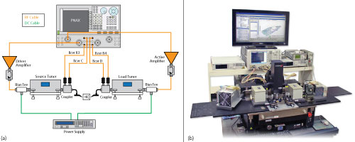
Figure 6 mmWave hybrid-active load-pull system (a) and setup (b).
Hybrid-active load-pull overcomes this limitation in the passive load-pull’s measurement range by adding an active injection signal to increase a2 and, therefore, increase Γ. A commercial hybrid-active load-pull system is shown in Figure 6a and a typical test setup in Figure 6b. The relationship between the transistor, the system impedance, the injection power and the tuning range is
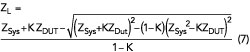
where ZL is the impedance presented to the DUT, ZSys is the system impedance and ZDUT is the DUT’s output impedance. K is defined as
where Pa2 is the active tuning power injected into the output of the DUT at the DUT reference plane, Pb2 is the DUT’s output power and Z0 = 50 Ω. The net reflection achievable at the DUT reference plane is
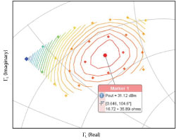
Figure 7 Hybrid-active on-wafer load-pull measurement of a GaN transistor at 30 GHz.
With a driver amplifier output of 40 dBm and using the same passive impedance tuner to transform the system impedance from 50 Ω to 23.17 + j28.12 Ω, it is possible to achieve Γ = 0.85 and successfully close the output power contours. The contours shown in Figure 7 demonstrate that a maximum output power of 31.12 dBm can be achieved by the same GaN transistor, which is 0.46 dB or approximately 11 percent more power than initially determined through passive load-pull with incomplete contours.
Conclusion
As companies accelerate development of 5G technologies and compete for best-in-class solutions, the optimization of power, efficiency and linearity will become more essential. Small advantages of a few dB in power or a few percentage points in efficiency may mean the difference between best-in-class and “never was.” Hybrid-active load-pull helps overcome the challenges in mmWave PA design by removing the uncertainty of unclosed contours. This enables ideal matching and gives those that adopt the methodology an edge in the marketplace.