
Limitations in Feed-forward Linearization: Part II
This article analyzes the effects of main path amplifier distortion characteristics on feed-forward systems. Part 1 ( Microwave Journal, August 2000) described the basic operation of a feed-forward amplifier system and the impact of nonideal effects on the ability of the system to linearize the main path amplifier. Part 2 describes the effects of large-signal nonlinearities and bandwidth limitations on feed-forward systems.
Fred Bonn
Motorola SPS, Wireless Infrastructure Systems Division
Tempe, AZ
Part 1 of this article introduced the operation of the basic feed-forward system. Using a small-signal or transconductance nonlinearity, the feed-forward system's ability to linearize in the presence of system gain and phase errors was analyzed. It was shown that while the perfect system would clean up any distortion, system-related gain and phase errors degraded linearization capability. It was also shown that error amplifier distortion degraded system performance. In Part 2 of the article, large-signal nonlinearities are introduced and their effects on the system are analyzed. Bandwidth limitations are also briefly discussed.
OTHER AMPLIFIER NONLINEARITIES
It was stated in Part 1 that simple transconductance nonlinearity is inadequate to describe the total nonlinear behavior of an amplifier. This fact is easy to see in Equation 1 of Part 1 as there is no limit on the output level. Physical limitations in the amplifier will eventually cause it to compress. There are several mechanisms at work that will cause the amplifier to compress. Current and voltage limiting are present as well as junction limiting and nonlinear reactance. Current and voltage limiting are straightforward and result more in clipping than compression. Limiting in device junctions such as the gate-source and base-emitter junctions result in typical compression characteristics. Nonlinear reactance can also cause the gain to fall off as the power level is increased because the matching network starts detuning as a result.
The change in reactance with power level also results in additional nonlinear behavior. The primary effect is spectral spreading as a result of reactance modulation. Some FM modulators use this method to create a frequency modulated signal.
It has been common practice to label spectral spreading as a result of nonlinear reactance modulation as amplitude-to-phase modulation (AM-PM) distortion and power-dependent nonlinear effects as amplitude-to-amplitude modulation (AM-AM) distortion. While not incorrect, these terms are ambiguous and cloud the effects in a veil of hocus-pocus. These terms are often bandied about to the point of losing all connection with physical basis. In this article, these terms will be avoided.
COMPRESSION EFFECTS

While there are multiple causes of amplifier compression, the net effect is a power-dependent transfer curve, as shown in Figure 1 . This curve represents the compression effects of only the fundamental term. A general transfer function representing the output voltage in the time domain is given by
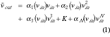
In this representation, the coefficients of the terms are input dependent. Analysis using Equation 1 would be rather unwieldly and is unnecessary. Remember that these series expansions are being used as tools to simplify the analysis of feed-forward systems and not to develop models for amplifiers. There are better methods for that. Only the first term in Equation 1 needs to be considered to gather a good understanding of what is important. Typical compression behavior is displayed and modeled using the hyperbolic tangent function (tanh), which is further broken down into a power series expansion as
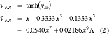
Again, this is not intended as an amplifier model but as an analytical tool to study the nonlinearity. Compression nonlinearity now has the same form as transconductance nonlinearity. Note that expansion in Equation 2 contains only odd-order components. Previously, it has been shown to expect odd-order intermodulation distortion (IMD) and spectral regrowth from this behavior. With all of the power concentrated in odd-order components, large spectral spreading as a result of compression effects is expected. The third-order coefficeint is particularly strong.
The plot uses a modified form of the series in Equation 2. Since only five terms are used in this alternating series, the last term was modified slightly to account for truncation effects. Figure 2 shows the spectral effects of the tanh function plotted via MATLAB. As expected, the output contains only odd-order distortion.

The tanh-like behavior of fundamental compression has been stated and the function shown to have only odd-order components. In reality, the compression characteristics only approximate a tanh function. Still, the compression characteristics contain a large odd-order characteristic, which dominates the response. Growth around the original tones is substantial as was expected from the odd-order characteristics. However, the distortion is largely input dependent, as seen from the transfer curve. At lower input levels, the function is almost linear. Despite the different characteristic in the nonlinearity, the feed-forward method is still capable of perfect linearization.
If the x-axis in the transfer curve plot is a voltage, then the 1 dB compression point occurs at an input voltage of 0.6125 V. Distortion generation can then be looked at relative to this point, as shown in Figure 3 . The amount of distortion created is shown to be input dependent and is a demonstration of the so-called AM-AM distortion. Amplifiers are often operated in a back-off mode relative to some compression level. The motivation for doing this is obvious from the transfer curve. While good for minimizing distortion, back-off operation results in less efficient operation.

Power amplifiers are often characterized for their output power and efficiency relative to meeting some spectral mask. There are some minor differences in the actual compression characteristics of different amplifiers that allow some to operate closer to compression (and thus higher efficiency and output power) while producing a minimum of distortion. Depending on the input signal type and method of measurement, there is also the possibility of operating in a "sweet spot." This point is where some measures of linearity such as third-order IMD start to improve or do not increase as much due to subtraction by phasing of higher odd-order IMD. Such characterization is rather dubious. The actual power-dependent transfer characteristics are much more indicative of true linearity. However, regardless of the characteristic of this nonlinearity, the idealized feed-forward method will remove the distortion.
POWER-DEPENDENT REACTANCE NONLINEARITY
In addition to compression effects, increasing input power will result in changes in amplifier reactance. This effect is primarily due to capacitance changes across pn junctions in semiconductor devices. The distortion resulting from this nonlinearity is generally referred to as AM-PM.
While there are several sources of varying capacitance in the active devices of an amplifier, a lot of insight can be gained by looking at a single gate-source junction of a GaAs MESFET amplifier. The nonlinear capacitance is given by

This equation also describes the gate-drain behavior. Gate bias keeps a reverse bias on the junction (VR ) at DC and low level AC signals, and the capacitance is primarily due to depletion layer effects. For large signal swings, the junction can become forward biased and diffusion capacitance may start to dominate. In this region, the capacitance increases rather quickly with voltage and Equation 3 is no longer valid. Although there is some change in gate-drain capacitance, it is not as dramatic as the gate-source component.
In an actual circuit the gate-source capacitance will be resonated out at the center frequency. The gate-source voltage swing is a function of input power and gate impedance. Figure 4 shows the relative phase shift of an ideal amplifier with a single nonlinear gate-source capacitance vs. a full three-stage laterally dif-fused metal oxide semiconductor (LDMOS) amplifier model as a function of power level. In the ideal amplifier, the junction capacitor is resonated at the center frequency with an inductor. Agilent's Advanced Design System (ADS) was used for this simulation. In the phase shift plot, the ADS symbolically defined device (SDD) is used to model the gate-source capacitance. This is a charge-based mathematical model for capacitance and not a diode; hence, there is no voltage limiting or compression as would be expected in a real diode. It should be noted that similar plots are sometimes called AM-PM plots. This nomenclature should be avoided since there is no spectral or modulation information in the plots. The displayed phase plot is a power-dependent phase graph.

Because there is no voltage limiting in the SDD implementation of the phase plot, the phase continues to advance with input level. The actual three-stage LDMOS model shows a leveling off in the phase at some input power. Figure 5 shows the SDD modified to include a diode I-V characteristic, and the phase is seen to limit at some power level. Remember in both of the plots that the ideal amplifier represents only one stage and one nonlinear capacitance. The LDMOS amplifier data have a steeper slope due to the multiple stages and multiple nonlinear reactances. Still, the behavior is similar, indicating the basic origin and limiting of power-dependent phase changes.

SERIES REPRESENTATION
OF JUNCTION CAPACITANCE
Representing the nonlinear capacitance in a series expansion has several problems. While generating the series for VR = Vo is rather easy, including the forward region approximation poses some problems because the function used is not continuous into the forward region. Even if this could be done, using the result is rather messy.
The nonlinear capacitance produces both amplitude and phase distortion. The variable reactance causes a node voltage change, which is amplitude-induced distortion. In a resonant circuit this will be Q dependent. If this amplitude variation as a function of drive voltage is modeled, then that function can be expanded into a series and used to predict distortion as before.
The phase change resulting from voltage-dependent reactance changes becomes more complicated. This is a phase modulation process that results in FM being generated and requires different and more complex analysis.
REACTANCE-DEPENDENT AMPLITUDE DISTORTION
The resulting AM modulation from reactance changes must be separated from pure reactance changes since the resulting spectral effects will be different. Simple phase vs. drive power functions such as that used in the ADS system amplifier will not capture the amplitude effects associated with nonlinear reactance. Signal bandwidth and circuit Q play a large role in determining what the ultimate spectral effects are. For typical low Q circuits in amplifiers and relatively low bandwidth signals, the effects of amplitude modulation may be minimal. In some cases, they could become a more significant factor.
SPECTRAL EFFECTS DUE
TO NONLINEAR CAPACITANCE
Two-tone Analysis
As demonstrated previously, two-tone testing is a good indicator of what to expect in spectral regrowth for digitally modulated signals. Figure 6 shows two-tone results from power sweeping a junction capacitance using ADS. Second-order IMD dominates with third-order a close second. Fourth-order IMD is significantly down and fifth-order does not appear. Thus, rather large close-in spectral spreading can be expected, but none farther out.

ACPR Reduction vs. AM-PM
Spectral regrowth due to phase modulation is shown in Figure 7 using ADS simulation. This particular simulation invokes diode limiting. As the phase shift increases due to increasing drive power, spectral regrowth increases. As limiting is approached, the regrowth levels off.

Most of the regrowth is confined close to the main lobe, as shown in Figure 8 . The regrowth due to phase modulation is much more narrow than that due to compression effects.

EFFECTS OF POWER-DEPENDENT PHASE SHIFT IN THE FORWARD LOOP ON CARRIER CANCELLATION
The power-dependent phase plots would indicate that a phase shift through the forward amplifier could cause an upset in the phase balance of the carrier cancellation circuit. Simulation demonstrated that not to be the case, as shown in Figure 9 . No other distortion effects are included. The phase shift in the main amplifier is treated as a form of voltage waveform distortion. It is detected via the input reference and developed as another error signal. Phase modulation in the main amplifier has no effect on the system. Phase modulation in the error loop appears as another source of distortion as described in Part 1.

BANDWIDTH CONSIDERATIONS
Thus far the system presented has not been subject to bandwidth limitations. This condition is unrealistic for all but the main amplifier. The output of the main amplifier has very limited bandwidth due to the matching components in the output circuit. This characteristic modifies (filters) the elements of Equation 1 in Part 1. These modified elements are still extracted by the carrier cancellation circuit. Remember that the feed-forward system does not care how the distortion was developed in the forward amplifier. In fact, the coefficients of Equation 1 (in part 1) can be modified to absorb any filtering. However, once the voltage waveform is sampled, the fidelity of the forward amplifier signal must be maintained to the output summation circuit. The error path must maintain the integrity of the error signal, which means it must have the same bandwidth as the error signal.
To avoid confusion about the effects of filtering on distortion, an important observation must be made. Amplifier distortion cannot be improved by filtering. This statement may appear to contradict the preceding paragraph, but it does not. Active devices for amplifiers are characterized in terms of their transconductance, which is a voltage-to-current transfer function expressed as
The output voltage can be filtered by providing a low impedance to the out-of-band currents. These currents still exist in the device drain or collector but are shorted to ground. These distortion currents still generate in-band distortion currents, which generate in-band voltage components. Shorting or filtering harmonic currents is a good practice since those voltages do not appear across the load. The transconductance nonlinearity that is voltage to current is unaffected by the choice of load impedance.
If this fact appears to contradict experimental evidence, consider the following. If a device is not unilateral, changing the load (or source) impedance can result in lower IMD measurements. In fact, a better measurement is all that was attained. In nonunilateral devices (and all are), feedback of low frequency even-order IMD results in mixing with the incoming signal to produce components that fall on odd-order IMD frequencies. Although parasitic feedback is generally low at low frequencies, if the termination impedance is high, a considerable amount of voltage feedback is possible. Coupled with the high gm at low frequencies, a considerable increase in two-tone IMD can be measured. Low impedance low frequency terminations prevent these voltages from appearing and a considerable measurement improvement can be made. The device transconductance nonlinearity does not change.
EFFECTS OF FORWARD AMPLIFIER BAND-LIMITING
Band-limiting can be introduced via filtering in the forward amplifier. Bandpass filtering is most appropriate as it coincides with the bandpass nature of most RF amplifiers. Another concern when considering band-limiting is amplitude variation within the passband. Figure 10 shows the effects of various bandpass filters in the forward path. Band-limiting and ripple in the main loop have no effect on linearization.

EFFECTS OF ERROR LOOP BAND-LIMITING
The error loop is quite sensitive to bandwidth limitations. Figure 11 shows a bandpass filter set up about the carrier frequency of 100 MHz with a 50 MHz bandwidth. There is no filtering in the main loop in this case. Even with this wide bandwidth, all of the even-order and out-of-band odd-order components will be filtered off. Linearization is severely degraded in this case. Error loop bandwidth may be the limiting factor in the feed-forward system's ability to linearize.

CONCLUSION
The performance of a feed-forward system falls mainly on system-level issues. The ideal feed-forward system, which has distortion in the main loop but behaves perfectly elsewhere, will produce an undistorted replica of the input signal. The nature and level of distortion in the main loop is irrelevant. This fact has been demonstrated both analytically and via simulation.
Gain and phase errors in the carrier cancellation circuit will cause serious degradation in the system's ability to remove distortion. This condition has been demonstrated both analytically and through simulation. Gain and phase errors must be tightly controlled in order to maximize the linearization process. There will always be static and dynamic phase and gain errors so the system will never behave perfectly.
In terms of amplifier quality, it is the error loop device that is most critical. It has been shown both analytically and through simulation that the quality of the output is directly related to the quality of the error amplifier. It is not that the imperfect error amplifier cannot remove the forward amplifier distortion, but the fact that it adds its own distortion to the output. A poor error amplifier can actually result in more distortion. The advantage in the error amplifier is that it only amplifies the distortion component, which is (hopefully) much lower in power than the desired component. For these reasons it is not possible to specify an error amplifier in terms of its ability to linearize. It will always linearize the distorted input and then add its own. All one can say is that as a result of Equation 11 in Part 1 the more linear the amplifier, the better.
Bandwidth issues were dealt with rather superficially. Bandwidth limiting in the main path is of no consequence. Although not expanded on in great detail, bandwidth limiting in the error path can be very serious. In fact, band-limiting in the error path may be the single greatest impediment to linearization in the feed-forward system. However, this premise has not been proven here. *
References
1. P. Kenington, Linearized RF Amplifier and Transmitter Techniques , Wireless Systems International Ltd. , 1998.
2. F. Zavosh et. al., "Digital Predistortion Techniques for RF Power Amplifiers with CDMA Applications," Microwave Journal , Vol. 42, No. 10, October 1999, pp. 2250.