
Mixers are essential RF front-end elements as they are responsible for translating a signal to a different frequency. They do this by beating (heterodyning) the signal of interest with another signal to produce an intermediate frequency. An ideal mixer produces the desired output signal with a clean spectrum, however practical mixers produce many unwanted spurious signals as well. Additionally, circuit parasitics and device nonlinearities generate further mixing spurs that limit system performance. Mixers can utilize various types of devices including diodes, FETs and BJTs, each with its own strengths and weaknesses.
Tradeoffs in conversion loss, LO drive, port-isolations, noise, VSWR and linearity are among the many aspects of mixer design. These parameters have a predominant influence on overall system performance, especially dynamic range. In particular, a highly linear mixer with low conversion loss and low distortion characteristics is a key desire for most system designs. This is where FET-based mixers have an advantage.
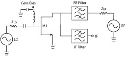
Figure 1 FET resistive mixer.
A FET-based mixer can be designed to operate in either an active or passive manner. In the active mode, the FET is typically DC biased as an amplifier, but with the gate near pinch-off. The LO and RF signals feed the gate, or gates if a dual-gate device is used, and the IF signal is coupled off the drain. This configuration provides gain, but at the cost of input compression and higher levels of intermodulation products. Passive resistive FET mixers, on the other hand, have conversion loss, but display outstanding input compression and intermodulation characteristics. This article focuses on the passive resistive FET mixer, covering its basic operation and design, concluding with measurements on a GaAs-based mmWave MMIC.
Basic FET Resistive Mixer Operation
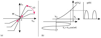
Figure 2 FET DC IV curves as the LO and RF swing about the linear region (a) and FET channel conductance modulation waveform (b).1
A FET resistive mixer utilizes the resistive channel between the drain and source of a “cold FET” or “unbiased FET” to achieve frequency translation. The RF input signal is applied across the drain-source channel of the FET, while the LO signal is applied to the gate. The IF output signal then appears across the drain. This configuration is shown in Figure 1, where a diplexer is needed to separate the RF and IF signals present at the drain.
It works by modulating the channel resistance at the rate of the applied LO signal, which produces the mixing action with the RF signal. During the positive cycle of the LO, the RF sees the linear resistance of the channel, as seen in Figure 2a, enabling it to achieve low intermodulation distortion levels. Figure 2b shows the operation of the mixer over time for a series of conductance pulses at the rate the LO is presented to the RF.
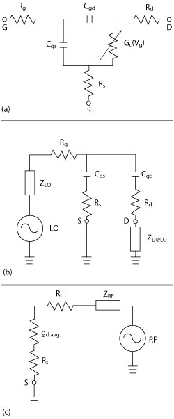
Figure 3 Nonlinear equivalent circuit with no drain bias (a), simplified equivalent LO circuit (b) and simplified equivalent RF/IF circuit (c).2
Matching
In Figure 3, ZLO represents the LO source impedance, to which is matched the gate impedance in order to maximize the voltage across capacitor Cgs. This can be done by considering the equivalent small signal model in Figure 3a. The LO input impedance depends mainly on the RC circuitry and can be reduced to the equivalent circuit shown in Figure 3b.2 The small signal RF and IF impedances are determined in a similar fashion, with the channel conductance replaced by the time-averaged value of the on-off variation over the LO cycle. Further refined estimates can be made by including the gate terminated by the gate impedance evaluated at the RF and IF frequencies. The simplification shown in Figure 3c is sufficient if the reactance of Cgd is large compared to the resistances of Rg and Rs.3
To prevent LO leakage from pumping the drain conductance through Cgd, the RF and IF matching circuit should ideally be designed to short-circuit the drain at the LO frequency (see Figure 3a). Also, the gate should be short-circuited at the RF frequency to prevent the RF voltage from varying the channel conductance.4
Topologies
Although the focus is on a single-ended FET mixer thus far, FET resistive mixers can be used in balanced topologies as well to further improve isolation and reduce intermodulation distortion (IMD). Figure 4a shows a single balanced topology with the LO applied to the gates through a balun and the RF applied to the drains in phase. Because the LO drives the two gates in a balanced (180 degree) fashion, the IF signals appearing at the drains are 180 degrees out of phase. These are filtered through a diplexer and recombined using an output balun. A key difference between the single balanced FET mixer and a single balanced diode mixer is the additional balun in the FET mixer; the extra balun is required to recombine the IF since, unlike diodes, the FETs cannot be operated in reverse. Single balanced configurations can achieve similar conversion losses as their single-ended FET mixer counterparts, but with a 3 dB improvement in odd-order IMD performance because of the RF power splitting between the two devices. The single balanced topology also has an inherent rejection of even-order IMD products due to the drains being shorted by the IF blocking caps. Depending on the quality of the balance, even order improvements of 20 dB or more can be achieved.4 Note that either the LO or RF can be applied out of phase, but generally the LO is chosen to be balanced, for in this configuration, the drains are a virtual ground to the LO, thus reducing the LO’s ability to pump the drain and cause further distortion.
Figure 4b shows a double balanced version in a ring structure; note that the extra balun is still required in contrast to a double balanced diode mixer. All four corners of the ring are virtual grounds for the LO and the IF connection points are virtual grounds for the RF. Both RF connections are made at virtual ground points with respect to the LO and IF. Thus, the RF, LO and IF are inherently isolated from each other in this configuration. This mixer also has the same IM rejection properties as a diode ring mixer; that is, all even order IM products are canceled out.5 Isolations and even order IM distortion products are both dependent on the quality of circuit balance maintained throughout the mixer.
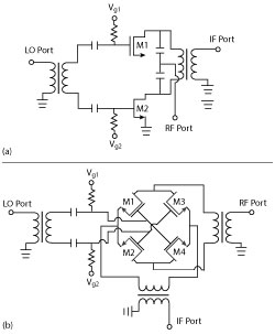
Figure 4 Balanced FET resistive mixer topologies: single balanced (a), double balanced (b).
Along with the desired IF signal, practical mixers generate an abundance of spurious products involving harmonics of the RF and LO. For instance, an input signal consisting of two distinct tones incident at the mixer results in IF products of various orders according to:

These products are generated by the nonlinearities in the device, similar to those of an amplifier. The key difference is that mixers have an additional signal, the LO which converts the intermodulation products to the IF frequency as seen in Figure 5a for the down-converting case. Figure 5a shows the two tones along with the close in third-order (n1 + n2 = 3) intermodulation products (IM3). Note that this occurs with all other harmonics of the LO present within the mixer as well, which are not shown. The extrapolated intercept of the fundamental and IM3 products when the RF input power is swept is shown in Figure 5b is called the output third-order intercept point (OIP3). The input third-order intercept (IIP3) is simply related to the OIP3 by the gain as OIP3 = IIP3 + gain. Achieving the highest possible IIP3 implies that the close-in IM3 are very small relative to the fundamental.
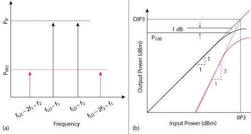
Figure 5 Mixer’s two-tone output spectrum at IF (a) and fundamental and IM3 levels vs. two-tone input power (b).