
Abstract
Recent developments within the high speed converter industry have enabled the fabrication of 28 nm process converters. The benefits of using smaller processes are many, especially for electronic warfare (EW) systems, where large bandwidth, high agility and low size, weight and power (SWaP) are required. These new capabilities also allow for the integration of multiple analog-to-digital converters (ADC) and digital-to-analog converters (DAC) within a single package. This integration reduces the power consumption compared to single ADC and DAC packages. By taking advantage of the smaller manufacturing process, the designer is able to create higher channel counts with an inherently radiation-hardened device, while achieving faster sample rates than converters manufactured using a larger geometry process.
Benefits of Using 28 nm and Lower Process Converters
As converter transistor sizes decrease, the parasitic gate capacitance is reduced, and converters are able to be operated at faster sample rates. These faster rates result in generally wider Nyquist bandwidths, enabling the broad instantaneous bandwidths required for EW systems. Additionally, smaller transistor size results in the ability to fit more transistors onto a given die, resulting in greater converter channel counts per package. Faster sample rates and greater channel counts provide the ability to achieve both the broad instantaneous spectrum sniffing and simultaneous multi-band interrogation required for signals intelligence (SIGINT) systems. Reduced feature sizes could potentially enable the integration of both a DAC and ADC core into a single monolithic package, creating the ability to design full-duplex EW transmitter and receiver systems with a single converter chip. Further, smaller transistor sizes allow for additional circuitry to be added to converter packages, such as numerically-controlled oscillators (NCO) and digital down-converters (DDC), to simplify the large digital signal processing (DSP) tasks required by EW systems. 28 nm processes lead to smaller cross-sections, usually resulting in fewer radiation-induced soft errors compared to similar features in a 65 nm process. The reduced damage from stray ionizing energy creates more robust electronic protect (EP) or electronic support (ES) systems.
28 nm Multi-Channel ADCs and DACs
Some potential benefits of integrating multiple converter channels among other components, such as NCOs and DDCs, into a single ADC and DAC package include reduced system power consumption and design-to-market time, faster transmitter/receiver calibration routines, simplified impedance-matching designs to a single package laminate and smaller physical footprints for EW systems. Analog Devices Inc. (ADI) is able to achieve these benefits by combining the company's state-of-the-art converter core design expertise with packaging experience to create multiple-channel, single-package ADC and DAC EW solutions.
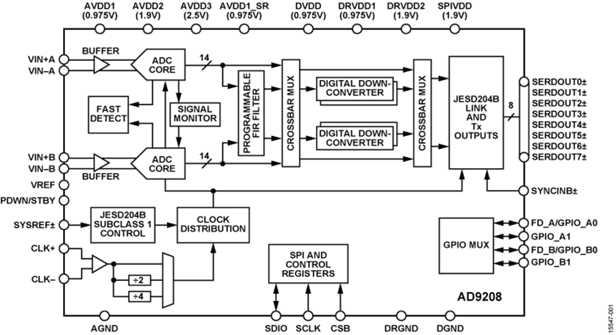
Figure 1 shows an example of this integration in the AD9208, a dual-channel, 14-bit, 3 GSPS ADC capable of sampling wideband analog signals up to 5 GHz. Its 28 nm process integrates wideband decimation filters, NCO blocks and DDCs to simplify EW receiver design. The on-chip NCOs and DDCs allow for lower digital data output rates, hence reduced power consumption, while still allowing the user to evaluate the entire captured spectrum.

Similarly, to ease EW transmitter designs, Figure 2 details the AD9172, which is a dual-channel, 16-bit, 12.6 GSPS RF DAC manufactured on a 28 nm process. In this case, integrated NCOs and interpolation filters allow for flexible, multi-band frequency planning and frequency synthesis up to 6 GHz. Dual-channel DACs create the ability to generate wideband in-phase and quadrature-phase (I/Q) complex data signals. In conjunction with the AD9208, the AD9172 can serve as the backbone for wideband, low power EW systems.
Summary
28 nm and smaller processes provide the ability to create either reduced footprint or more dense EW systems, increasing channel counts and/or instantaneous bandwidths. These smaller processes enable single-package, multi-channel ADCs and DACs to create robust EW solutions with fewer baseband interfaces. This integration at Analog Devices, Inc. is enabling many customers to compete in the EW landscape.