
A novel approach for the design of broadband high efficiency power amplifiers (BHPA) simplifies the process of synthesizing a wideband output matching network by realizing harmonic tuning and fundamental matching separately. First, the second and third harmonic load impedances are calculated based on the theory of the continuous class F mode. Then, a novel wideband harmonic suppression network is obtained by using microstrip radial stubs (MRS) that is unaffected by the adjacent fundamental matching circuit. A power amplifier (PA) designed with a 10 W Wolfspeed GaN HEMT device achieves a fractional bandwidth of 30.4 percent from 1.95 to 2.65 GHz, with 60.9 to 81.6 percent drain efficiency (DE), 60 to 79.9 percent power-added efficiency (PAE) and 39.7 to 41.7 dBm output power across the operating band. As shown through the design process, simulation and measured results, this approach makes the design of the harmonic load network easier and more accurate compared to existing methods, for which it is difficult to simultaneously control the fundamental and harmonic impedances, especially at higher frequencies. This method can be widely applied to BHPA design for modern wireless communication systems.
Besides linearity, a major concern in PAs today is the improvement of output power and efficiency across a wide bandwidth, to meet the demands of expanding communication networks and increasing data rates in various wireless standards such as GSM, WCDMA, WIMAX and LTE. For the PA modes so far considered, the switch-mode PA (SWPA) has attracted considerable research attention due to its high performance with respect to output power and conversion efficiency. Class F mode in the SWPA achieves high efficiency with nonoverlapping square wave voltage and half-sinusoidal current drain waveforms at the output of the active device. In this simple way, the class F mode PA has become one of the most cited.1-3
For practical reasons, finite harmonics (typically the second and third) are controlled by λ/4 transmission line resonators to approximate the proper harmonic load impedances. This method, however, inevitably results in an output matching network with a high Q factor. Consequently, the inherent narrowband performance (typically less than 10 percent) of a class F amplifier is difficult to overcome and limits its potential for wideband applications. Some pioneering work4-6 provides several good approaches for expanding the bandwidth of the class F mode PA, but its limitations can only be moderately overcome.
An extended PA mode, derived from class J PAs and known as the continuous class F7, demonstrates a great advantage in terms of high efficiency across a broad band. In the continuous class F case, amplifiers can achieve high output power and efficiency delivered by class F through various combinations of voltage and current. Only the current waveform needs to be constant, and the voltage waveform is no longer just a square wave, but a collection of waveforms.
The output matching impedance is generally controlled up to the third harmonic. The third harmonic remains in the open state and the second harmonic on the impedance Smith chart runs along the R = 0 circle, while the fundamental wave impedance is on a resistance circle moving in the opposite direction. Taking parasitic elements such as drain capacitance and bonding wire inductance into consideration, the situation compared with the ideal will change at different frequency points. Actually, the continuous class F mode provides a series of solutions for optimal fundamental and harmonic matching impedance across a wide frequency band.
The design described here employs a new architecture addressing the difficult harmonic control problem (up to the third harmonic). In the output network, MRSs are used to obtain precise harmonic impedances, while fundamental impedances are achieved with stepped impedance transformers.
THEORY
In a class F mode PA, the drain voltage and current are shaped into nonoverlapping square and half sinusoid waves, respectively, by shorting the even harmonics and presenting an open to the odd harmonics. Typically, only second and third harmonic control is taken into account in a practical design because of small improvements in efficiency with greater circuit complexity when higher harmonics are considered. The normalized, optimum drain voltage waveform with a corresponding efficiency of 90.7 percent8 is expressed as:
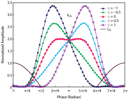
Figure 1 Continuous class F voltage and current waveforms.

The above equation represents a voltage waveform that must be tuned precisely at the current generator plane of the device; therefore, a class F PA is usually implemented for maximum power and efficiency at a single frequency. Efficiency degrades quickly for frequencies outside the operating band.
The continuous class F mode provides formulas for a series of waveforms to overcome the class F mode bandwidth limitation. The waveforms for providing high power and efficiency can be obtained by introducing a varying parameter, γ, to the voltage waveform formula. Its modified voltage waveforms can be described as:

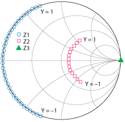
Figure 2 Theoretical continuous class F mode impedance curves, showing the fundamental and second and third harmonic loads.
Voltage waveforms for the case γ = 0 turn into the standard class F mode. The continuous class F mode can maintain the performance of its counterpart, class F, by changing the standard class F drain voltage waveform as the parameter γ varies over the range -1 ≤ γ ≤ 1. This leads to a family of voltage waveform solutions. In this way, the corresponding maximum normalized drain voltage amplitude increases from 2 to 3.37 (see Figure 1), sustained by utilizing GaN device technology. It can be seen that when γ = 0, the waveform corresponds to the class F case.
In practice, harmonic impedances must be calculated from the following equation:

where n represents the order of the harmonic component. Ropt is defined as the optimum impedance for the standard class B mode, expressed as:

Vdc is the drain bias voltage, Vknee is the knee voltage of transistor and Imax is the maximum drain quiescent current. The drain current waveform of the continuous class F PA is the same as that of the class F mode PA, which is based on a Fourier series expansion and defined as:
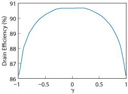
Figure 3 Efficiency degradation vs. γ.

The corresponding impedance is determined by equations 2, 4 and 5 as follows:


Figure 4 Equivalent circuit of the Wolfspeed CGH40010F GaN transistor.
The nature of the impedance curves for -1 ≤ γ ≤ 1 is shown in Figure 2. The third harmonic impedance remains in an open state and the second harmonic impedance moves along the R = 0 circle of the Smith chart, while the fundamental impedance moves in the opposite direction.
CONTINUOUS CLASS F PA DESIGN
Figure 2 shows that in an ideal case the third harmonic impedance is constrained to be infinite; however, this is extremely difficult to achieve and is not necessary for a practical design. In this article, a simple and practical approach is described for obtaining the harmonic impedances. Through the action of a nonlinear device output capacitance, CDS, as discussed by Tutly, et al.,9 the third harmonic high efficiency impedance trajectory is made to move along the edge of the Smith chart. This can be done by harmonic load-pull after the second harmonic termination is determined. The position of the γ = 0 point should be noted. This method of third harmonic load determination guarantees a high efficiency BHPA design.

Figure 5 Continuous class F output matching network layout.
From Equation 2, the fourth harmonic impedance is also important in the continuous mode; however, design of a broadband continuous class F PA with fourth harmonic control is difficult and will inevitably require a very complicated circuit. The more feasible method is to neglect the fourth harmonic impedance. The effect of neglecting Z4f on continuous class F performance can be calculated. The result is shown in Figure 3 as the parameter γ is varied. Degradation in efficiency is less than 4.5 percent over the range of γ values. The maximum degradation occurs at γ = +1, which can be avoided by limiting the bandwidth.
Limitation of Bandwidth
The target bandwidth should be limited to avoid overlapping with the harmonic bandwidth. The target fundamental band is set from

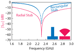
Figure 6 Comparison of a radial vs. rectangular stub.
and the second and third harmonic bands can be expressed as follows:

As previously discussed, control of the fourth harmonic is neglected. From Equation 7, bandwidths overlap when

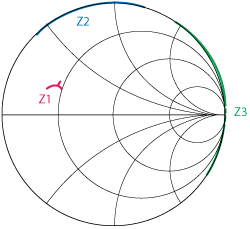
Figure 7 Impedance of the continuous class F output matching network, showing the fundamental (Z1), second (Z2) and third (Z3) harmonic components.
Equation 8 represents the overlapping case for the fundamental and second harmonic bands. Equation 9 represents the overlapping case for the second and third harmonic. For the ideal continuous class F PA where the third harmonic is in an open state, consider the overlapping of the fundamental and second harmonic bands represented by Equation 8. The fractional bandwidth (FBW) of the ideal continuous class F is

It is clear that the limitation of Equation 9 is more restrictive than the limitation of Equation 8. The FBW from Equation 9 is:
Load Impedance with Parasitic Parameters
In a practical design utilizing a packaged GaN device, as described here, parasitic parameters must be taken into account. The parasitic model of the Wolfspeed CGH40010F GaN device is shown in Figure 4.10
Due to the impact of parasitics, the load impedance reference plane of the continuous class F PA shifts from the ideal current generator plane to the package plane. This forms a fundamental impedance area and a harmonic impedance area. These areas correspond to a series of solutions. The key to a successful design is to contain the matching load impedances in these areas, respectively, across a wide band. As a consequence, the voltage waves do not strictly follow the variation shown in Figure 1.
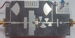
Figure 8 Fabricated BHPA.
Output Matching Network
In this architecture, MRS are used for harmonic control and stepped impedance transformers are used for fundamental matching over a specified range of frequencies. Commercial computer-aided design (CAD) software is used for greater accuracy in determining the harmonic impedances presented to the device. The output matching network used for the continuous class F design is shown in Figure 5.
As Figure 6 shows, a radial stub exhibits wider bandwidth performance and a much deeper resonance than a rectangular stub. More important, however, is that the four radial stub structure can realize a constant 0 Ω resistance over a wide band. In other words, it forms a stable structure that is independent of the fundamental matching network. This harmonic network is the key to separating the harmonic terminations from the fundamental matching. In addition, the structure of up-and-down radial stubs is convenient for fabrication, avoiding overlap when the second and third harmonic matching stubs are closely spaced.
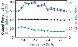
Figure 9 Measured performance of the BHPA.
The corresponding target loads and behavior of the output matching network (fundamental and second and third harmonic) are shown in Figure 7 over a band from 1.95 to 2.65 GHz. It is apparent that the second and third harmonic components behave in accordance with the design requirements.
BHPA FABRICATION AND MEASUREMENT
The design is implemented on a Rogers 5880 substrate with εr = 2.2, a dielectric thickness of 0.787 mm and a copper thickness of 18 µm (see Figure 8). The Wolfspeed CGH40010F GaN HEMT packaged device has a drain bias of 28 V with a corresponding quiescent drain current of 168 mA. Large-signal continuous wave (CW) PA characterization is conducted from 1.95 to 2.65 GHz. The results in Figure 9 show PA performance in terms of output power, gain, drain efficiency and PAE as a function of frequency. The prototype achieves 39.7 to 41.7 dBm output power and a peak PAE of 60 to 79.9 percent with 30.4 percent bandwidth, extending from 1.95 to 2.65 GHz. The highest PAE is 79.9 percent, but it is nearly impossible to maintain this level throughout the entire operating band (in the upper part of the band, PAE drops to 60 percent).
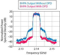
Figure 10 BHPA output spectra for a 5 MHz WCDMA signal with and without DPD.
A 5 MHz WCDMA signal is used to evaluate linearity and adjacent channel power ratio (ACPR) characteristics at 2.14 GHz. The BHPA output spectra with and without digital predistortion (DPD) are shown in Figure 10. The PA achieves an average drain efficiency of 32.1 percent and an output power of 35.3 dBm. The ACPR is -32.8 and -32.7 dBc at ±5 MHz offset, and -50.5 and -50.9 dBc at ±10 MHz offset. After applying DPD, the ACPR significantly improves to -49.7 and -48.6 dBc at ±5 MHz offset, and -59.0 and -55.6 dBc at ±10 MHz offset.
CONCLUSION
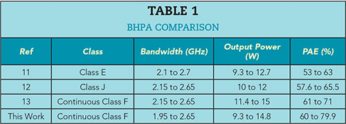
A novel method for synthesizing an output matching network consists of a four MRS harmonic control structure and a stepped impedance fundamental matching structure. This method provides an easy approach to BHPA design. A BHPA is implemented using a GaN HEMT over an operating frequency band of 1.95 to 2.65 GHz. Its performance compares favorably with a selection of current state-of-the-art designs shown in Table 1. Analysis shows that the second harmonic is matched well for high efficiency and output power. The theory of third harmonic impedance matching is extended for practical broadband design to mitigate the fact that a fixed third harmonic load (as defined for the continuous class F mode) is extremely difficult to implement over frequency. Test results show that this structure can achieve high efficiency and power gain across a 1.95 to 2.65 GHz band. Linearity improvement is achieved with DPD.
References
- P. Colantonio, F. Giannini, G. Leuzziand and E. Limiti, “On the Class-F Power Amplifier Design,” International Journal of RF and Microwave Computer-Aided Engineering, Vol. 9, No. 2, March 1999, pp. 129–149.
- Y. Y. Woo, Y. Yang and B. Kim, “Analysis and Experiments for High Efficiency Class-F and Inverse Class-F Power Amplifiers,” IEEE Transactions on Microwave Theory and Techniques, Vol. 54, No. 5, May 2006, pp. 1969–1974.
- P. Colantonio, F. Giannini and E. Limiti, High Efficiency RF and Microwave Solid State Power Amplifiers, John Wiley and Sons, 2009.
- D. Kang, J. Choi, M. Jun, D. Kim, J. Park, B. Jin, D. Yu, K. Min and B. Kim, “Broadband Class-F Amplifiers for Handset Applications,” Proceedings of the European Microwave Conference, September 2009, pp. 1547–1550.
- A. N. Stameroff and A. V. Pham, “Wide Bandwidth Inverse Class-F Power Amplifier With Novel Balun Harmonic Matching Network,” IEEE MTT-S International Microwave Symposium Digest, June 2012, pp. 1–3.
- A. Garcia-Osorio, J. R. Loo-Yau and J. A. Reynoso-Hernandez, “A GaN Class-F PA With 600 MHz Bandwidth and 62.5 Percent of PAE Suitable for WiMAX Frequencies,” IEEE International Microwave Workshop Series on RF Front-Ends for Software Defined and Cognitive Radio Solutions, February 2010, pp. 1–4.
- V. Carrubba, A. L. Clarke, M. Akmal, J. Lees, J. Benedikt, P. J.Tasker, S. C. Cripps, “The Continuous Class-F Mode Power Amplifier,” Proceedings of the European Microwave Conference, September 2010, pp. 432–435.
- S. C. Cripps, RF Power Amplifier for Wireless Communication, 2nd edition, Artech House, Norwood, MA, 2006.
- N. Tutly, L. Guan, A. Zhu and T. Brazil, “A Simplified Broadband Design Methodology for Linearized High-Efficiency Continuous Class-F Power Amplifiers,” IEEE Transactions on Microwave Theory and Techniques, Vol. 60, No. 6, June 2012, pp. 1952–1963.
- P. J. Tasker and J. Benedikt, “Waveform Inspired Models and the Harmonic Balance Emulator,” IEEE Microwave Magazine, Vol. 12, No. 2, April 2011, pp. 38–54.
- M. P. van der Heijden, M. Acar and J. S. Vromans, “A Compact 12-Watt High-Efficiency 2.1-2.7 GHz Class-E GaN HEMT Power Amplifier for Base Stations,” IEEE MTT-S International Microwave Symposium Digest, June 2009, pp. 657–660.
- N. Tuffy, A. Zhu and T. J. Brazil, “Class-J RF Power Amplifier with Wideband Harmonic Suppression,” IEEE MTT-S International Microwave Symposium Digest, June 2011, pp. 1–4.
- N. Tuffy, A. Zhu and T. J. Brazil, “Novel Realisation of a Broadband High-Efficiency Continuous Class-F Power Amplifier,” Proceedings of the European Microwave Integrated Circuits Conference, October 2011, pp. 120–123.