
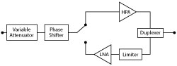
Figure 1 Generic T/R module.
Phased array radars have several advantages over conventional radars that use rotating antennas: phased arrays can transmit multiple beams simultaneously, place a null in the direction of a side-lobe jammer and can have a planar or conformal topology. Phased arrays can be one, two or three dimensional, but in every case they consist of an array of individual antenna elements with each element driven by a transmit/receive (T/R) module. In the simplest case of a passive phased array, the T/R module consists of just a cascade of a phase-shifter and an attenuator which are adjusted for each element to steer the beam, with a passive feed network connecting the T/R modules to a central transmitter and receiver.
However, the full benefits of a phased array radar are not realized in this case since the losses of the feed network, particularly for an array with many elements, significantly degrades the system noise figure and transmitter output power. For the best performance it is necessary to use a fully-active T/R module which has both a low noise and high power amplifier located inside it. Numerous different architectures have been proposed for a T/R module but Figure 1 shows a basic generic one.
Until recently, most solid-state phased arrays have used GaAs MMICs for the high power amplifier (HPA), but the advent of GaN on SiC transistors and MMICs, with their higher efficiency and power output, means that most solid-state radars in the future will use GaN. However, there are two issues that need to be considered when using GaN on SiC in a T/R module, one economic and the other technical. Dealing with the economic issue first, GaN on SiC is more expensive than GaAs. This arises from the use of smaller substrate sizes (4" typically for GaN compared with 6" for GaAs), and because the substrate is SiC rather than GaAs. A large fraction of a GaN HPA MMIC real estate is occupied by the passive circuit elements rather than the active device, which exacerbates the cost issue. Various solutions to this problem have been proposed such as realizing all of the passive circuitry on separate GaAs substrates and butt-joining them to the GaN transistor power bars.1 At X-Band and above there really is no alternative to the use of either a pure GaN MMIC or a hybrid GaN/GaAs MMIC solution since the elements’ size requirements cannot be greater than λ/2 apart (to prevent grating lobes),2 which means that there is no space for any form of packaged device.
However, at S-Band and below it is possible to consider the use of packaged devices such as a conventional pre-matched GaN on SiC transistor or a transistor that is fully matched to 50 Ω inside the package. It is this latter solution which forms the focus of this article, and the economic benefits for the radar manufacturer will be shown.
The technical issue associated with using GaN on SiC transistors in T/R modules arises from the fact that they have a very high power density, which limits the VSWR withstand capability. A glance at the datasheet of any commercially available pulsed GaN on SiC transistor will quickly show that the VSWR withstand capability is typically in the 3:1 to 5:1 range, but it is well known that the T/R modules will see a poor VSWR at some beam directions due to mutual coupling3 between the antenna elements. If a T/R switch is used as the duplexer in the T/R module then this poor VSWR will be applied directly to the GaN HPA less any improvement arising from the insertion loss of the T/R switch itself, and this can lead to HPA failure.
Using a three-port circulator, as the duplexer does not help much either since the limiter will reflect all of the power directly into the HPA, again less any improvement arising from the insertion loss of the circulator. It might be thought that the solution to this VSWR withstand problem is to use a balanced amplifier. While balanced amplifiers have several advantages such as presenting excellent input and output terminal VSWRs even when designed for lowest noise figure or maximum output power, it is readily shown4 that they do not offer any improvement to the VSWR withstand capability. A solution to the poor VSWR withstand capability of GaN is to use a non-reflective limiter such as a four-port circulator.
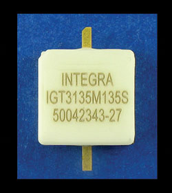
Figure 2 S-Band (3.1 to 3.5 GHz) 135 W GaN transistor internally matched to 50 Ω. Package size is 0.4" × 0.4".
TRANSISTORS MATCHED TO 50 Ω
Transistors that are fully matched to 50 Ω are 100 percent tested at full rated output power by the transistor manufacturer under the exact pulse length and duty cycle conditions that the radar requires. This is difficult if not impossible to do with MMICs using an RF-on-wafer probe tester when the power exceeds a few watts. Furthermore, fully matched transistors can be supplied in gain and phase matched blocks if required. Assembly costs are also reduced compared with using MMICs since only one assembly operation is required, namely solder attach of package and leads which can both be undertaken at the same time, whereas MMICs require solder die-attach first followed by wire bonding. T/R assembly yield is also higher since with MMICs the wire bonds form part of the matching network whereas in a 50 Ω transistor the matching is all contained within the package.
T/R assembly yield is also higher since tuning is eliminated compared with using pre-matched transistors. In effect, some of the assembly, tuning and manufacturing costs associated with producing a T/R module are passed from the T/R module manufacturer to the transistor manufacturer and this is reflected in a slightly higher price for a fully matched transistor compared with a standard pre-matched one. Figure 2 shows an example of a 135 W S-Band transistor that is internally fully matched to 50 Ω.
Transistors fully matched to 50 Ω also have several other advantages compared to MMICs. For example, it is quick and easy to alter the frequency range or the power output of the device if required, whereas for a MMIC a new mask set is required followed by a new wafer fabrication, both of which make it expensive and time-consuming. The bond wires used as inductors in the matching networks have much higher Q than the distributed components used in MMICs, which results in less power loss and higher efficiency.
Another key advantage is that U.S. government export restrictions are much less severe for a 50 Ω transistor than a MMIC. For example, in S-Band radar applications in the 3.1 to 3.5 GHz band, the maximum power output for a MMIC is restricted to 40 W if an EAR99 classification is required, whereas for a 50 Ω transistor the limit is 115 W. Finally, although a packaged 50 Ω transistor is clearly larger than a bare MMIC, that disparity is largely eliminated when comparing packaged MMICs with a 50 Ω transistor. For comparison the 50 Ω transistor shown in Figure 2 measures 0.4" × 0.4" whereas a packaged MMIC such as Qorvo TGA2813-SM for the same frequency range has outside dimensions of 0.35" × 0.28". The MMIC part only delivers 100 W saturated output power whereas the 50 Ω transistor delivers 150 W saturated output power. Admittedly, the MMIC is a two-stage amplifier and so has more gain.
OPTIMUM LOAD IMPEDANCE
If 100 W per element is required in the phased array, then no matter whether a MMIC or discrete transistor is used for the HPA, the output device will require to see a resistive load of 12.5 Ω at the internal current generator plane based on standard load-line theory of V2/2P for a GaN device operating from a typical drain voltage of 50 V.5 This is the load impedance that is required for maximum linear output power (i.e., no waveform clipping) for a transistor that has a constant value of gm for all values of gate-source voltage above the threshold voltage.
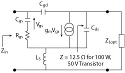
Figure 3 Simplified equivalent circuit of a GaN transistor. For a 100 W, 50 V S-Band transistor, typical values are Cgs = 30 pF, Cgd = 1 pF, Cds = 9.6 pF, gm = 4 S, Rgs = 0.45 Ω, Ls = 0.03 nH.
The above analysis also assumes a transistor without any source inductance, feedback capacitance or output capacitance. Real transistors of course have all three elements present and this modifies the load impedance that must be connected to the transistor to achieve the same output power. An analytic expression has been derived6 for the optimum load for a transistor with finite values for Ls, Cgd and Cds and is given by:
where RLopt is the value for optimum load impedance for the situation where Ls, Cgd and Cds all have zero value, i.e., 12.5 Ω in this case. Figure 3 shows a simplified equivalent circuit for a GaN transistor. The source of the transistor can be connected to ground with bond wires or via holes but, regardless of which method is used, the transistor will have a finite value of source inductance.
A 3D electromagnetic analysis was performed of the grounding structure for the transistor shown in Figure 2, which showed that Ls =0.03 nH. Even though 0.03 nH has a reactance of only 0.57 Ω at 3 GHz, it will be shown that this is the dominant effect controlling the value of the transistor’s input impedance. Using the values for these elements given in Figure 3 then ZLopt at the drain terminal of the die is now a 10.7 Ω resistor in parallel with an inductance of 0.20 nH instead of just a pure 12.5 Ω resistor. Transforming the external 50 Ω load down to 12.5 or 10.7 Ω requires only a 4:1 impedance transformer, which is relatively easy to implement, the problem lies in trying to place a shunt inductor of value 0.20 nH immediately adjacent to the transistor die and the fact the package inherently forces a series inductance to be present in front of the 10.7 Ω load.
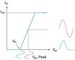
Figure 4 Voltage and current waveforms for ideal class A and B amplifiers.
For these reasons transistor manufacturers normally work with a series load configuration with the first element being the inevitable series drain bond wire inductance. For the transistor being considered here then transforming the parallel RL load to a series, one requires that the device sees a load impedance of 1.75 Ω in series with a 0.20 nH inductor. The transformation of 50 Ω down to 1.75 Ω requires a 25:1 impedance transformer which is much harder to realize. For the transistor being described here this is achieved using a series LCL matching network inside the transistor package, and this network transforms the external 50 Ω load resistance down to ZLopt and so no matching is required on the PCB, i.e., the external RF circuit is simply a 50 Ω transmission line with a drain bias network attached.
CLASS OF OPERATION
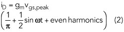
Transistors designed for radar applications are invariably operated in almost pure class B with the transistor conducting for only half of the RF cycle (Idq < 50 mA for the example shown) rather than class A. Figure 4 compares the class A and B situations. Fourier analysis of the current waveform in Figure 4 for class B operation shows that the drain current is given by:
while in class A the drain current would be simply:

Comparing Equations 2 and 3 shows immediately that gm must be replaced by gm/2 in Equation 1 for class B operation.
Although the transistor is biased in almost pure class B mode as far as DC is concerned, it is questionable whether it actually operates in the classical class B mode from an RF point of view. Fourier analysis of the drain current waveform shows that it has components at DC, the fundamental frequency and at even harmonics of the fundamental frequency. The harmonics must be terminated in a short-circuit in order to have a pure sinusoidal output. For a transistor with a large output capacitance then this requirement is satisfied by the transistor’s own internal output capacitance.
For the transistor under consideration Cds = 9.6 pF so the output capacitance presents a reactance of 2.8 Ω to the second harmonic rather than a short-circuit. Also, the transistor has an LCL low-pass network connected to the drain pad on the die to provide some pre-matching inside the package, which will also present a reactive impedance to the second harmonic. Without access to device waveform measurement data it is difficult to be precise on exactly how the transistor operates, but this does not invalidate the general conclusions about the input impedance that are discussed next.
INPUT IMPEDANCE
The resistive part of the input admittance Yin has both an intrinsic and an extrinsic component. The intrinsic component is a result of the finite value of gate-source resistance Rgs in Figure 3, which is comprised of the source Ohmic contact resistance and the channel resistance formed by the GaN layer between the source contact and the depletion region under the gate. However, the channel resistance in a GaN transistor is extremely low since the electrons flow in a two-dimensional electron gas. For the 135 W S-Band GaN transistor shown in Figure 2, Rgs is in the region of 0.45 Ω. However, since 1/ωCgs>> Rgs it will be shown in what follows that the value of Rgs makes very little contribution to the overall value of the resistive part of Yin as it is masked by the much larger reactance of the gate-source capacitance.
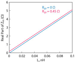
Figure 5 Computed value of the real part of Zin vs. source inductance Ls when terminated in ZLopt, given by Equation 1.
The extrinsic contributor to the resistive part of the input admittance Yin arises from the finite value of the gate-source feedback capacitance, Cgs, and source inductance, LS, which cause a portion of the resistive load impedance to appear at the input. If the effect of Rgs is ignored for the reason just given, and it is also temporarily assumed that Ls = 0, then straightforward circuit analysis shows that the input admittance with an arbitrary value of load resistance RL connected at the output is given by:
Since 1>>(ωCgdRL)2 then this expression simplifies to:
The reactive term is, of course, the well known Miller effect6 whereby the effective input capacitance is not simply Cgs + Cgd but the increased value Cgs +(1+gmRL)Cgd. However, since gm must be replaced by gm/2 in Equations 4 and 5 for class B operation, the Miller effect is halved in class B compared with class A. This fact doesn’t seem to be mentioned in most books and articles on RF amplifier design. The factor of two reduction in the gm value for class B operation is also the reason why class B amplifiers have less gain (theoretically 6 dB lower but not quite as bad as that in practice) than class A amplifiers.
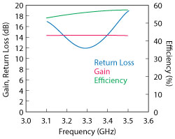
Figure 6 Measured performance of the Integra Technologies IGT3135M135S transistor, with Idq = 25 mA, Vds = 46 V, a 300 µs pulse length and 10% duty cycle.
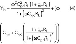
For a transistor with finite values of both Cgd and Ls it has been shown6 that the input impedance when terminated in ZLopt is given by:
The optimum source impedance is simply the complex conjugate of Zin. It can be seen immediately from Equation 6 that the real part of Zin is linearly dependent on the value of source inductance, thus controlling its value is critical to obtain a high production yield for a transistor fully matched to 50 Ω at the input. Figure 5 shows the computed value of Zin as a function of the value of source inductance for the situation where Rgs = 0 and Rgs = 0.45 Ω. It can be clearly seen that the finite value of gate-source resistance makes very little difference to the value of the real part of Zin which justifies the earlier assumption that it can be neglected in the analysis.
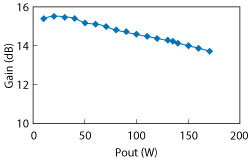
Figure 7 Gain vs. output power for the IGT3135M135S transistor, with Idq = 25 mA, Vds = 46 V, a 300 µs pulse length and 10% duty cycle.
To match a transistor having a real part of Zin in the region of 1.5 Ω (the measured value is actually a lot less than this) to 50 Ω over the frequency range 3.1 to 3.5 GHz entirely within the package is a daunting task. It requires a matching network with more sections than the simple three-section one used at the output. Figure 6 shows the input return loss and associated gain across the band. The data is taken with a fixed output power of 135 W. The typical input return loss is better than 12 dB across the band with 14 dB gain and >55 percent drain efficiency.
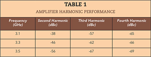
Figure 7 shows the gain vs. output power from which it can be seen that the transistor is operating at 1 dB gain compression at 135 W output power. Finally, the harmonic performance is given in Table 1. Incorporating lumped element matching within the package at both input and output helps to suppress harmonics and is a major advantage compared with using external distributed matching. The harmonic performance given in Table 1 is better than would be achieved with a MMIC that uses on-chip distributed matching.
CONCLUSION
This article described the economic and technical benefits of using a transistor fully matched to 50 Ω rather than a MMIC in T/R modules used in phased array radars. Values for the impedances at the gate and drain terminals of the transistor die have been given and, despite the fact that the resistive part of the input impedance is about 1 Ω, it has been shown that it is still possible to produce a transistor that is matched to 50 Ω over a 400 MHz bandwidth centered on 3.3 GHz with an input return loss better than 12 dB.ν
References
- Merv Haynes, Alistair Bullen, David Hone and Dilbagh Singh, “Overview of GaN Technology Applications within Finmeccanica,” Proceedings of ARMMS Conference, Thame UK, April 18-19, 2016.
- Merrill L Skolnik, “Introduction to Radar Systems,” McGraw-Hill, Second Edition, pp. 281.
- Merrill L Skolnik, “Introduction to Radar Systems,” McGraw-Hill, Second Edition, pp. 306.
- John L.B. Walker, “High-Power GaAs FET Amplifiers,”Artech House, pp. 294–6.
- S.C. Cripps, “A Method for the Prediction of Load-Pull Contours in GaAs MESFETs,” Proceedings of IEEE International Microwave Symposium, 1983, pp. 221–3, 1983.
- John Walker, “Analytic Expressions for the Optimum Source & Load Impedance and Associated Large-Signal Gain of an RF Power Transistor,” Proceedings of IEEE International Microwave Symposium, Philadelphia, June 8–13, 2003, pp. 1725-8.