
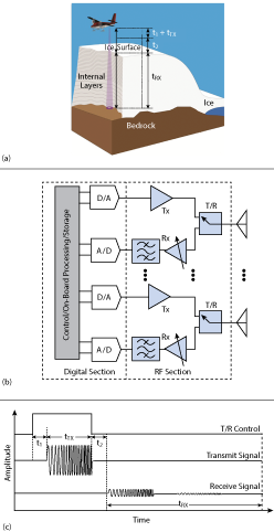
Figure 1 Airborne coherent multichannel ice sounding radar operation (a) simplified block diagram (b) and timing diagram (c).
High-power transmit/receive (T/R) switches for use in multi-channel ice-penetrating imaging radars are capable of sustaining peak power levels exceeding 1000 W. They are based on a balancedtopology and built using quadrature hybrids and actively biased PIN diodes. Insertion loss is lower than 1.3 dB from 100 to 350 MHz and lower than 1.6 dB from 150 to 600 MHz. Isolation in transmit mode is higher than 85 dB across both bands with turn-on and turn-off times shorter than 1300 ns and 200 ns, respectively. Both designs were successfully used in multi-channel radars for measurements in the Arctic and Antarctic.
Airborne ice penetrating radars are widely used for measuring ice thickness and mapping the internal structure of glacial ice.1 Recent advances in RF and high-speed digital technologies have contributed to the development of multi-channel radars for imaging the ice-bedrock interface and sounding the most challenging areas of ice sheets, such as fast-flowing glaciers and ice sheet margins.1-3
The configuration of a multi-channel airborne coherent radar with transmit/receive (T/R) capabilities is illustrated in Figure 1. The radar RF section is composed of multiple, identical channels interfaced to a digital back-end as shown in Figure 1a. Alternating between T and R modes is accomplished using a high-power T/R switch. During transmission the switch connects the antenna to the transmitter with minimal power loss and isolates the receiver. During reception, the switch connects the antenna to the receiver and isolates the transmitter. The radar timing diagram is shown inFigure 1c. The switch is toggled using a digital signal (denoted T/R control). Switching speed requirements for this application are driven by the nominal aircraft flight altitude of 500 m above the surface. This corresponds to a round-trip travel time of 3.3 µs. To maximize receiver dynamic range, the radar is operated with a combination of short (1 µs) pulses and long (3 to 20 µs) pulses. The short pulses sound the ice surface and map shallow internal layers, and the longer pulses sound the ice-bedrock interface and map deep internal layers. For 500 m altitude and 1 µs pulses, the T/R switch must be capable of fully transitioning between “on” and “off” states in less than 2.3 µs while preserving adequate power handling, isolation and insertion loss.
Recent implementations of ice sounding radars with T/R capabilities employ narrow bandwidth systems with relatively low average power. These include, for example, the single-channel 60 MHz system with 4 MHz bandwidth and 1.5 W average power (600 W of peak power at 0.25 percent duty cycle) demonstrated by Christensen et al.,4 and the 2-channel 60 MHz radar with 15 MHz bandwidth and 22.4 W of average power per channel (3.2 kW of peak power per channel operating at 0.64 percent duty cycle) demonstrated by Peters et al.5
We explored a variety of commercial off-the-shelf (COTS) and custom solutions for the T/R switches for our radars. Initially, we used a COTS single pole double throw (SPDT) switch based on positive-intrinsic-negative (PIN) diodes with a built-in driver. This approach rendered a fully functional system, but suffered from a slow switching time (2.4 µs turn-on, 4.2 µs turn-off), limited peak power handling capability (250 W) and bandwidth (100 MHz), and relatively high cost. (Cilla-Hernandez, et al.,6 developed a 90 W PIN diode switch with 100 MHz bandwidth for a UHF ice-penetrating radar. They also pointed out the lack of COTS switches with high power handling and fast switching characteristics.) Next, we employed a high-power ferrite-based circulator in combination with a medium power gallium nitride (GaN) switch. This reduced the switching time to about 50 ns but restricted the bandwidth of the system to that of the circulator (30 MHz). More recently, a wideband duplexer based on the circuit proposed by Cofrancesco et al.,7 was demonstrated employing medium-power silicon (Si) epitaxial planar diodes without active biasing.8 This configuration had outstanding switching speed and bandwidth performance—less than 50 ns and 300 MHz, respectively—but its peak power was restricted to 250 W.
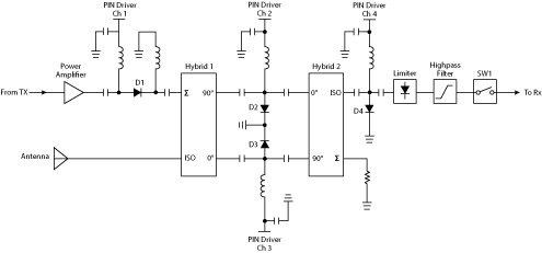
Figure 2 T/R switch simplified block diagram based on a balanced duplexer configuration.
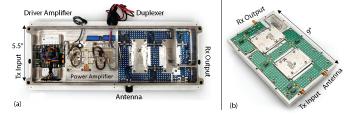
Figure 3 100 to 350 MHz T/R module integrated with a driver amplifier, 1 kW power amplifier and PIN diode drivers (a) 150 to 600 MHz T/R switch integrated with PIN diode drivers (b).
To further improve radar performance, we increased the peak transmit power to about 1 kW per channel. This required developing the circuit presented in this paper. This new design replaces the Si diodes in the balanced topology with high-power PIN diodes individually biased using a custom driver circuit. (The balanced duplexer topology with active diode biasing was implemented earlier for radar and nuclear magnetic resonance applications9,10 employing bandwidths ranging from 6 MHz to 25 MHz and peak power levels up to 150 kW. None of these implementations were wideband or fast enough for our application, primarily due to the technology limitations of their time.) First, we developed a prototype that operates in the 100 to 350 MHz range. This design was integrated into a set of compact modules that were then incorporated into a radar on the NASA DC-8 aircraft as part of a NASA Operation IceBridge (OIB) mission in the Antarctic.11 A second and final design was developed for use in a radar operating over the 150 to 600 MHz band. The new radar was operated on a NASA C-130 aircraft as part of OIB to collect data over the Arctic sea ice and the Greenland ice sheet.
Design Description
Figure 2 shows a simplified block diagram of the T/R switch circuit. It consists of a pair of wideband 90 degree hybrids connected back-to-back; a series PIN diode switch element (D1: Cobham Metelics MEST2G-150-20); and three shunt switch elements (D2-D4: Cobham Metelics MSWSH-100-30). Diodes D1 and D2-D4 can handle up to 150 W and 300 W average, respectively. Each diode is biased individually via RF chokes, using a multi-channel custom driver that accepts standard TTL levels from the digital system. The driver is based on the standard BJT-based configuration widely available in the literature.12,13 The switching speed is improved by means of a Baker-clamp circuit and by optimizing the lumped components and PCB layout. For the 100 to 350 MHz configuration, we chose the QH8100 90 degree hybrid from Werlatone Inc., while the QH8840 was chosen for the 150 to 600 MHz configuration.
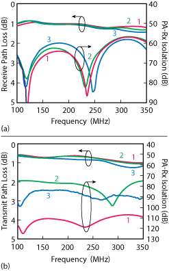
Figure 4 Circuit simulation (1), EM and circuit co-simulation (2) and measured small-signal S-parameters (3) for the 100 to 350 MHz module receive (a) and transmit (b) states.
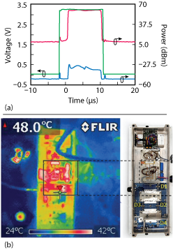
Figure 5 100 to 350 MHz T/R switch during high power operation, showing transmit signal envelope (red) and feedthrough signal envelope (blue) with a high power, 10 μs RF pulse (a) infrared image of the temperature distribution on the module top face (b).
During transmission, the T/R control is set to “high” and PIN diodes D1-D4 are forward-biased with 100 mA. The RF output from the power amplifier is injected into the sum port of the first hybrid through the series diode D1, reaching shunt diodes D3 and D2 with in-phase (I) and quadrature (Q) components. D2 and D3 present a reflective impedance to the I-Q signals, which are re-combined at the isolated port of Hybrid 1. This results in a low-loss path between the power amplifier and the antenna. Diode D4 and the limiter (Cobham Metelics LM200802-M-A-300) are used to protect the receiver from RF leakage. The switch SW1 is added to increase isolation and reduce video feedthrough from the PIN diodes. During reception, the T/R control is set to “low” and the diodes are reverse biased at VR = -12 V. High voltages are not required since only low-power RF signals are present in this state. The signal from the antenna is split equally by Hybrid 1 then recombined into the isolated port of Hybrid 2, resulting in a small power loss between antenna and receiver. The diode D1 is added to increase receive isolation. A low-loss high-pass filter is placed between the limiter and isolation switch SW1 to reduce low-frequency transients from PIN diode switching. The receiver section is enclosed in a separate cavity to further increase isolation to the transmitter.
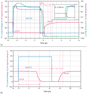
Figure 6 Measured switching characteristics of two T/R switches: internal design with an inset showing the turn-off time (a) commercial switch used in the earlier version of the radar, showing much slower switching speed (b).
For the 100 to 350 MHz version, the high-power switch is integrated with a 1 kW power amplifier and a 10 W driver amplifier. The power amplifier is based on a reference design for the MRFE6VP61K25H from NXP.14 The driver amplifier is a two-stage design based on Polyfet RF Devices modules. For the 150 to 600 MHz design, the power amplifier is housed on a separate chassis. Figure 3 shows photographs of both designs. The PIN diode drivers are located at the back of each module (not shown).
Experimental Results and Discussion
Small-Signal Simulations and Measurements
The design is first verified over the 100 to 350 MHz range using Keysight’s Advanced Design System (ADS) with S-parameters provided by the manufacturers for all the components, including the PIN diodes. To increase the model accuracy, first-order layout effects are considered by incorporating microstrip and coplanar transmission line sections and junctions. The PCB layout for the RF section is accomplished in CadSoft Eagle and imported into ADS for EM/circuit co-simulation. Both transmit and receive modes are simulated and then measured using a 4-port vector network analyzer. The results are presented in Figure 4.
In receive mode, the circuit simulation, EM/circuit co-simulation, and measured results show excellent agreement. The insertion loss between the antenna and receiver ports is less than 1.3 dB with less than 0.15 dB deviation between simulations and measurements. Further, the simulations accurately predict more than 57 dB of isolation between the power amplifier port and the receiver port of the switch. In transmit mode, the circuit and EM/circuit co-simulation yield an expected 0.7 to 0.9 dB of insertion loss between the antenna and the power amplifier ports. The measured insertion loss agrees with simulation to within 0.16 dB. The design target for isolation between the transmitter and receiver in this mode is 70 dB. The circuit simulation overestimates this, predicting a value greater than 105 dB across the band, while co-simulation predicts it to be at least 75 dB. The discrepancy between the two simulated results is expected, because the circuit simulation includes only first-order effects of the PCB layout. Measured isolation is 87 to 96 dB; this exceeds design requirements, but differs from the simulation. The difference between the co-simulated and measured result is due to the fact that the rectangular cavity enclosing the receiver section of the duplexer is not included in the simulation. Similar performance is obtained for the 150 to 600 MHz design in both transmit and receive modes, with a slight increase of insertion loss in the upper part of the band when in the receive mode (1.6 dB max without including the loss of SW1).
Large Signal Measurements
To verify the power handling capability of the circuit, we excite the high-power amplifier chain with the radar waveform generator. The latter is set to produce both single-tone and chirped pulse signals over the frequency range of the current antennas on the NASA DC-8 (165 to 215 MHz). Figure 5shows the measured envelope of transmit and feedthrough signals after calibrating for losses in the test setup. Note that the TTL control signal (shown in green in Figure 5a) has a slight time offset to allow the amplifiers to fully turn on before RF power is applied. The measured output power is about 60 dBm across the band. The feedthrough signal ranges between -27 and -36 dBm, which confirms 87 to 96 dB isolation. The highest temperature in the circuit was observed across the series diode D1 (TJmax= 175°C), as shown in Figure 5b.
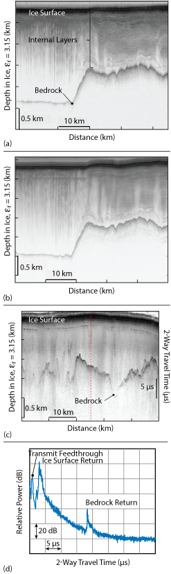
Figure 7 Radar echograms obtained in Antarctica with an earlier version of the radar (a) data collected over the same area using the new 100 to 350 MHz switch design (b) data collected using the new 150 to 600 MHz switch (c) A-scope showing the relative received power (at the location identified with the red dotted line in (c) as a function of travel time (d).
Switching Time
To verify the circuit switching speed, we inject a low-power CW tone into the antenna port of the circuit while toggling T/R control. We monitor the voltage across the PIN diodes and the signal at the receiver port. The RF pulse duration is set to 1 µs with a PRF of 15 kHz. The top inset of Figure 6ashows the measured results, indicating a very fast transition from 50 percent TTL to 10 percent RF at the receiver port (200 to ns turn-off time). The transition from 50 percent TTL to 90 percent RF at the receiver port occurs in 1300 ns (turn-on time). These values include driver delays (450 ns max). Figure 6bshows measured results for a COTS switch used in previous versions of our radars. Its turn-off time is 4.2 µs (21 times slower than our circuit) while its turn-on time is 2.4 µs (almost 2 times slower than our circuit).
Sample Radar Results
We used the 100 to 350 MHz and 150 to 600 MHz switches in two radars employed for extensive collection of ice thickness data over the Antarctic and Arctic. The 100 to 350 MHz design, integrated as a set of six T/R modules, was operated over the 165 to 215 MHz band onboard the NASA DC-8. Figure 7b shows sample results using the system that incorporates this design, with a 50 MHz bandwidth and 6 kW of total peak transmit power (6 antennas). The echogram was obtained after synthetic aperture radar (SAR) processing and displays the relative received signal intensity in a dB scale as a function of depth and geographic location.
We also include an echogram from data collected over the same area using a lower-power, narrow bandwidth system deployed in 2010 (see Figure 7a). This system employed 10 MHz bandwidth COTS T/R switches with close to 1 kW of total peak transmit power (5 antennas). See Gogineni, et al.,2 and F. Rodriguez-Morales, et al.,3 for further details on the radars and the processing techniques applied to obtain these products. The wider bandwidth and increased transmit power of the new system results in improved resolution and signal-to-noise ratio (SNR), respectively. We estimate an overall SNR improvement of 10 to 14 dB.
The 150 to 600 MHz design was recently tested onboard the NASA C-130H aircraft operating over Southeast Greenland using a two-element antenna array with a 270 MHz bandwidth and close to 2 kW of total peak transmit power. Figures 7c and 7d show field-processed results from data obtained exercising the T/R switches over the 180 to 450 MHz range. The lower limit of this band is set by the antenna response, while the upper limit is set by the waveform generator. Recent improvements to the digital system will allow us to exercise the entire 150 to 600 MHz bandwidth.
Conclusion
Fast, high-power T/R switches and modules for a multi-channel ice imaging radar are capable of handling over 1 kW of peak power (150 W average) with demonstrated switching speeds faster than 1300 ns, including up to 450 ns of driver delays. Two different circuits, operating at different frequency bands, were validated in the laboratory and in the field. Sample radar results show the enhanced performance obtained through the higher power and wider bandwidth enabled by these modules. Future work includes the incorporation of faster PIN-diode driver circuits, further miniaturization and increasing peak power.
Acknowledgments
This work was supported by the NSF (grants ANT- 0424589 and 1229716) and NASA (grant NNX10AT68G). The authors would like to thank R. Hale, P. Place, B. Townley, D-Gomez-Garcia, A. Awasthi, S. Yan, A. Mahmood, A.R. Harish, E. Arnold, Z. Wang, B. Camps-Raga, J. Lyle, J. Citrolo, R. Crowe and M. Lowe for their contribution and support.
References
- C. Allen, “A Brief History of Radio Echo Sounding of Ice, Earthzine,” Piscataway NJ, 2008.
- S. Gogineni, J.B. Yan, J. Paden, C. Leuschen, J. Li, F. Rodriguez-Morales, D. Braaten, K. Purdon, Z. Wang, W. Liu and J. Gauch, “Bed Topography of Jakobshavn Isbrae, Greenland, and Byrd Glacier, Antarctica,” Journal of Glaciology, Vol. 60, No. 223, November 2014, pp. 813–833.
- F. Rodriguez-Morales, S. Gogineni, C. J. Leuschen, J. D. Paden, J. Li, C. C. Lewis, B. Panzer; D. Gomez-Garcia Alvestegui, A. Patel, K. Byers, R. Crowe, K. Player, R. D. Hale, E. J. Arnold, L. Smith, C. M. Gifford, D. Braaten and C. Panton, “Advanced Multifrequency Radar Instrumentation for Polar Research,” IEEE Transactions on Geoscience and Remote Sensing, Vol. 52, No. 5, May 2014, pp. 2824–2842.
- E. L. Christensen, N. Reeh, R. Forsberg, J.H. Jørgensen, N. Skou and K.A. Woelders, “A Low-Cost Glacier-Mapping System,” Journal of Glaciology, Vol. 46, No. 154, August 2000, pp. 531–537.
- M.E. Peters, D.D. Blankenship and D.L. Morse, “Analysis Techniques for Coherent Airborne Radar Sounding: Application to West Antarctic Ice Streams,” J. Geophysical Research Atmospheres, Vol. 110, No. 6, June 2005.
- C. C. Hernandez, V. Krozer, J. Vidkjaer, and J. Dall, “Design and Performance of an Airborne Ice Sounding Radar Front-End,” Microwaves, Radar and Remote Sensing Symposium, September 2008 pp. 284–288.
- P. Cofrancesco, G. Moiraghi, P. Mustarelli and M. Villa, “A New NMR Duplexer Made With Quadrature Couplers,” Measurement Science and Technology, Vol. 2, No. 2, 1999.
- Z. Wang, S. Gogineni, F. Rodriguez-Morales, J.B. Yan, R. Hale, J. Paden, C. Leuschen, C. Carabajal, D. Gomez-Garcia, B. Townley, R. Willer, L. Stearns, S. Child and D. Braaten, “Wideband Imaging Radar for Cryospheric Remote Sensing,” Proceedings of the 2014 IEEE International Geoscience and Remote Sensing Symposium, July 2014, pp. 4026–4029.
- N. Brown, “Design Concepts for High-Power PIN Diode Limiting,” IEEE Transactions on Microwave Theory and Techniques, Vol. 15, No. 12, December 1967, pp. 732–742.
- J. T. Vaughan, D. N. Haupt, P. J. Noa, J. M. Vaughn and G. M. Pohost, “RF Front End for a 4.1 Tesla Clinical NMR Spectrometer,” IEEE Transactions on Nuclear Science, Vol. 42, No. 4, August 1995, pp. 1333–1337.
- J. Li, J. Paden, C. Leuschen, F. Rodriguez-Morales, R. D. Hale, E. J. Arnold, R. Crowe, D. Gomez-Garcia and P. Gogineni, “High-Altitude Radar Measurements of Ice Thickness over the Antarctic and Greenland Ice Sheets as a Part of Operation Ice Bridge,” IEEE Transactions on Geoscience and Remote Sensing, Vol. 51, No. 2, February 2013, pp. 742–754.
- J. F. White, “Microwave Semiconductor Engineering,” Van Nostrand Reinhold Company, New York, 1982.
- C. Brorsson, “PIN Diode Drive Circuits Optimized for Fast Switching, Master of Science Thesis,” Department of Microwave Design, Chalmers University of Technology, Sweden, 2011.
- NXP, “VHF Digital TV Broadcast Reference Design,” http://cache.freescale.com/files/rf_if/doc/support_info/RDMRFE6VP61K25H_VHF_BCAST.pdf?fsrch=1&sr=5&pageNum=1.