
Identify Friend or Foe (IFF) and Secondary Surveillance Radar (SSR) systems are, from a hardware point of view, essentially the same system although the application is different. The radar systems developed in World War II could determine the range and bearing of aircraft but could not distinguish between friendly and hostile planes. IFF systems were developed at the same time to solve that deficiency.
The basic concept is illustrated in Figure 1. Although today’s systems are digital rather than analog and the frequencies used are different, the basic concept shown in Figure 1 has not changed. A ground-based transmitter sends out an interrogating pulse, which today is at 1030 MHz, to the aircraft. On receipt of this pulse the aircraft on-board transponder sends back a reply at a different frequency of 1090 MHz which, if it is a friendly aircraft, will contain a coded message that identifies it as a friendly aircraft. Thus IFF systems are basically military in nature. Further details about IFF and SSR systems can be found in1-3.
Civil aviation has a different need to the military, requiring information such as the aircraft’s flight number, its altitude etc. The basic difference between the military and civil uses of the IFF system is the information that is sent back to the ground station in the return pulse at 1090 MHz. Civil aviation labels this system a Secondary Surveillance Radar, but this is a misnomer since the returned pulse contains a data stream containing information about the flight, so in reality it is a communication system rather than a radar system. Nevertheless, it is universally termed an SSR and so this nomenclature will be used in this article. Figure 2 shows a typical SSR system co-located with the S-Band primary radar system which is used to detect any object in the path of the radar beam.
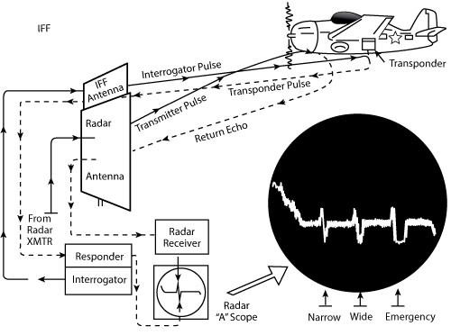
Figure 1 Principle of an IFF system. Source: Radar Bulletin 8A, U.S. Navy, 1950.

Figure 2 Airport co-located primary and secondary radar system. The SSR radar antenna is at the top with the S-Band antenna immediately beneath it. (Photo courtesy of Shutterstock.com).
SSR message formats have evolved over the years and the system that is in the most widespread use today is the Mode S version which transmits a train of 128 pulses of 0.5 µs on, 0.5 µs off with a long term duty cycle of 1 percent. As far as transistors are concerned, this is a very benign pulse train from a thermal point of view and any transistor technology can easily withstand this. However, a newer version of Mode S is being implemented called Extended Length Message (ELM) which uses a 48 pulse burst of 32 µs on, 18 µs off (i.e., 67 percent duty cycle within the pulse) with a long-term duty cycle of 6.4 percent.
As far as the transistor is concerned the off period during the pulse burst is not long enough for the transistor to fully cool down so from a thermal perspective the ELM Mode S pulse train looks like a 2.4 ms pulse with an overall duty cycle of 6.4 percent. This very long effective pulse means that the transistor is running close to CW conditions and many of the early generations of high-power pulsed RF transistors cannot be run CW without substantial de-rating.
This has necessitated the redesign of many SSR systems. The typical output power of a SSR transmitter is around 4 kW for the ground station while the airborne transponder is lower power at 1 to 2 kW. There is no requirement for linearity and so the transistors are often operated at about 2 dB into compression which helps achieve high efficiency.
The following is an assessment of the merits and disadvantages of silicon bipolar, silicon LDMOS and gallium nitride HEMT technologies for this application.
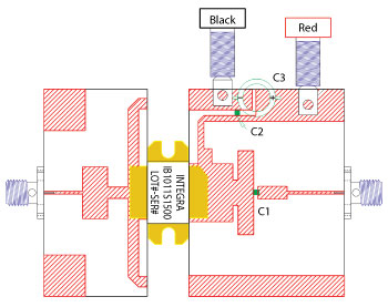
Figure 3 Circuit for IB1011S1500 1.5 kW Si bipolar junction transistor for SSR applications.
SILICON BIPOLAR TRANSISTORS
Early solid-state SSR systems used Si bipolar junction transistors (BJT) as this was the only transistor technology available and BJT-based SSRs are still being manufactured today. In fact, the standard mode S waveform3 suits the characteristics of BJTs very well because the thermally benign waveform enables full advantage to be taken of the high power density capability of a BJT. With a requirement for around 4 kW of output power, the ‘holy grail’ for an SSR manufacturer has been a transistor with an output power of at least 1 kW since then it is easy to combine four of these devices to achieve 4 kW.
In fact, a little more than 1 kW is needed to allow for losses in the combiner and the insertion loss of the isolator used at the output to protect the transistor from a high VSWR mismatch. BJTs fulfill this requirement nicely with devices up to 1.5 kW4. BJTs for this application are always operated in Class C mode with no applied DC voltage to the base-emitter junction and the typical efficiency is about 60 to 65 percent for a 1 kW device.
BJTs have the simplest RF circuitry of any technology. Figure 3 shows the circuit for the 1.5 kW 1030 MHz BJT, just two capacitors are used on the PCB plus a large external reservoir capacitor that is common to all types of transistors. It also only requires a single positive supply voltage.
BJTs also have one other extremely important attribute that is not enjoyed by either GaN HEMTs or LDMOS transistors. BJTs are operated in Class C so that when there is no applied RF pulse the transistor does not pass any DC current. Consequently, BJT-based SSRs inherently emit almost zero shot noise in the off period. LDMOS and GaN HEMTs, on the other hand, are always biased Class A/B and so emit shot noise in the off-period which is injected into the receiver along with the returned signal from the aircraft transponder causing receiver de-sensitization.
The required quiescent current for LDMOS and GaN is roughly proportional to the output power of the transistor so it is more of an issue for the kW-level transistors used in SSR systems than in low power systems. The solution to this problem is to use more complex DC circuitry which shuts down the transistor completely in the off-period but which turns the gate bias on ahead of the RF pulse5.
BJTs can also be designed for the ELM version of mode S, but the maximum output power drops to about 500 W due to thermal limitations. This means that a minimum of 8 BJTs are needed for a complete SSR. This has serious size and cost implications for the system. Thus, although BJT technology is well-proven and extremely reliable it is unlikely that any new systems will be designed using BJTs.
BJTs also have three other disadvantages, namely they use environmentally unfriendly BeO packages which are also expensive, and they have much lower gain than either LDMOS or GaN HEMTs which means that more gain stages are needed in the amplifier which, of course, adds to size and cost. Finally, the VSWR withstand capability for a 1 kW device is normally specified at 3:1 which means that the device needs to be protected by a high power isolator which also adds to the overall cost.
SILICON LDMOS
Silicon LDMOS became the main technology for communications and basestations in the mid 1990s, and it has since become widely accepted for L-Band avionics and radar applications, not least because it can be manufactured in a standard 8" CMOS wafer fabrication facility resulting in lower cost than bipolar RF power transistors. Also, kW-level LDMOS transistors are readily available that can withstand a 20:1 VSWR mismatch and this leads to a further system-level cost reduction since the expensive isolator that needs to be added at the output of a bipolar transistor amplifier can be eliminated.
A 1 kW LDMOStransistor typically has about 10 dB more gain than the corresponding BJT device so fewer driver stages are needed leading to further cost and size reduction. 1 kW LDMOS transistors are available in both single-ended and push-pull formats. Single-ended versions have simpler, smaller and cheaper circuits than push-pull versions since no balun is needed.
While the above highlights the plus points of LDMOS, there are also a couple of negative features. Firstly, since LDMOS is always operated in Class A/B rather than the Class C used by BJTs, the efficiency of an LDMOS amplifier is typically 5 to 10 percent lower than is achieved with a bipolar-based transmitter, usually in the mid 50 percent range. It is worth examining why the efficiency is much lower than the theoretical 78.5 percent that an ideal Class B amplifier would have. Class A/B bias is used as a compromise between the best gain which occurs in Class A but which has the worst efficiency, and Class B which has the best efficiency but the lowest gain. This fact alone accounts for a few percentage points reduction in the maximum efficiency from 78.5 percent which would occur in an ideal class B amplifier without any waveform clipping.
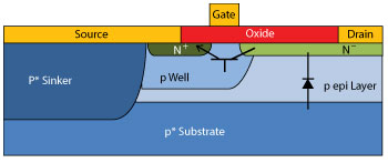
Figure 4 Parasitic bipolar transistor inside every LDMOS device.
However, it was mentioned earlier that the transistors in an SSR are typically operated about 2 dB into compression. This is very beneficial in terms of increasing the power output, if this didn’t happen then to get 1 kW would require an even larger and more expensive transistor but, as Cripps6 has shown, this also gives rise to another small reduction in efficiency.
A 1 kW transistor operated from a 50 V supply requires that the current generator in the transistor sees a load resistance of 502/2*1000 Ω ( /2PoutΩ) if full voltage modulation occurs, i.e., the transistor has zero on-resistance or knee voltage. Thus the transistor needs to see a load of 1.25 Ω but the RF path from the plane of the current generator to the external 50 Ω load is bound to have some series resistance, even 0.1 Ω would cause the efficiency to be reduced to 90 percent of its theoretical maximum value, for example, the ideal Class B efficiency would fall to 70 percent maximum.
All of the above efficiency-reduction mechanisms apply equally well to both GaN and LDMOS, but the next issue is more of a problem for LDMOS than GaN. Real transistors always have a finite on-resistance or, equivalently, knee voltage. This prevents full voltage modulation from occurring and leads to a further efficiency reduction7. GaN HEMT devices have a lower on-resistance for the same output power than LDMOS, and so do not suffer from this efficiency reduction mechanism to the same extent. Taken together, it is easy to see why all these efficiency degradation mechanisms result in LDMOS 1 kW transistors operated in Class A/B have typical efficiencies in the low to mid 50 percent range regardless of whether they are push-pull or single-ended.
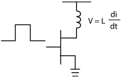
Figure 5 The drain bias inductor creates a voltage spike under pulsed operation.
The obvious solution to achieve better efficiency is to use one of the very high efficiency modes such as Class E or F, but this is where LDMOS is at a distinct disadvantage compared with GaN. These high efficiency modes all involve non-sinusoidal waveforms which mean that the output matching circuit must present a specific impedance to the transistor not just at the fundamental frequency but at the harmonics as well. In the case of Class F it is required that the circuit presents a very high impedance to the transistor’s internal current generator at odd-order harmonics and a short-circuit to even-order harmonics. Conversely, for Inverse Class F, a short-circuit to odd-order harmonics and an open-circuit to even-order harmonics is needed. However, the output capacitance of a 1 kW LDMOS transistor is so high that the harmonics are shorted to ground by the transistor’s own internal capacitance so that it isn’t possible to present the required high impedance needed for either Class F or Inverse Class F operation.
The second issue with LDMOS is that it has an inherent and unfortunate attribute, namely there is an unwanted parasitic bipolar transistor inside every LDMOS device. Figure 4 shows where this is formed in an
LDMOS device. Early LDMOS devices had a checkered start when first tested for high-power pulsed applications with devices failing. The problem was soon diagnosed8 as being caused by latch-up of the parasitic bipolar transistor under fast rise and fall times associated with pulsed operation. Invariably, the drain bias to the transistor is applied via an inductor as shown in Figure 5, but under fast rise and fall times a large enough voltage spike can be generated via L di/dt action to turn-on the parasitic bipolar transistor and cause device failure.
The higher the power of the transistor, the higher is the value of the di/dt term and so high power transistors are more prone to this problem than low power devices. Manufacturers have devised proprietary methods of reducing this effect, but in truth these techniques merely suppress the problem rather than eliminate it. Device failures can still occur if the rise/fall time is fast enough.
GaN HEMT TRANSISTORS
GaN HEMT devices use SiC substrates rather than Si substrates which greatly add to their cost, and the much smaller wafer size (4" versus 8") exacerbates the cost issue still further. Although GaN devices are moving to 6" SiC substrates, there will still be a cost penalty for using GaN. However, there is a mitigating factor; GaN HEMT devices have a much higher power density than LDMOS and so the die size is a little smaller for a given output power — but nowhere near enough to fully compensate the smaller size and higher cost of the substrate. Consequently, GaN must offer substantial performance advantages compared with LDMOS to justify its use in this application, so what are these advantages?
Probably the single most significant advantage is the much lower capacitance per watt that GaN HEMTs offer compared with LDMOS. This much lower capacitance is a consequence of the much greater power density (capacitance is proportional to gate periphery so if the same power is achieved from a smaller periphery then you get lower capacitance). The greater power density of GaN is often cited as its greatest advantage, but this is a very debatable attribute. The high power density creates thermal problems, especially in CW applications, which is why the GaN epitaxial layer has to be grown on SiC substrates rather than Si for high power transistors since SiC has a four-fold higher thermal conductivity than Si.
Consequently, the higher power density attribute is actually a cost driver. However, the low capacitance per watt has several very desirable consequences. Firstly, it enables higher power transistors to be produced. In pulsed applications, the fundamental limit on how much power a transistor can deliver is not set by thermal limitations but on the ability of the output matching network to transform an ever-lower output impedance to 50 Ω. At first sight it might be thought that GaN HEMTs have no advantage over LDMOS in this regard since RL=/2PoutΩ is identical for both types of transistor if operated from the same supply voltage — ignoring any difference in the maximum voltage modulation that each transistor can accommodate. However, all transistors have a finite output capacitance and this forms the first element in the output matching network. Hence the matching network external to the transistor has to transform not RL to 50 Ω, but RL in parallel with Cds to 50 Ω. The bandwidth over which it is possible to match RL in parallel with Cds is limited by Fano’s law9, RL becomes lower and Cds becomes higher as the power output increases and so the usable bandwidth of the transistor becomes smaller as the power increases.
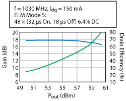
Figure 6 Gain and efficiency with harmonic tuning for IGN1030L1000.
The lower capacitance of GaN enables much higher power transistors to be produced than is possible with LDMOS, 1 kW devices10 are already commercially available and 1.5 to 2 kW devices will shortly be released. In fact, the limit on the power output from GaN under pulsed conditions is set not by the impedance but on the availability of a suitable package to fit all the GaN die inside.
The low capacitance per watt also results in higher efficiency. It was mentioned in the LDMOS section that the high output capacitance of the device results in all harmonics being terminated in a short-circuit within the transistor die itself. This is just what one wants for Class B operation but not what is needed if you want to use one of the higher efficiency modes such as Class F. The recommended circuit for the device shown in Figure 6, for example, presents a specific impedance to the transistor at the second harmonic to increase the efficiency.
The fact that the efficiency can be increased by altering the value of impedance at the second harmonic implies that the capacitance within the GaN chip is sufficiently low that the second harmonic is not being completely shorted within the die itself. Figure 6 shows a graph of gain and efficiency versus output power from which it can be seen that the typical efficiency during the pulse under Mode S ELM operation at 1 kW is 80 percent, about 25 percent higher than is achieved using LDMOS, and better even than is achieved with a Class C BJT. The 1 kW output power is achieved at 1 dB gain compression. A further advantage of GaN HEMTs over LDMOS is the lower on-resistance, or knee voltage if you prefer that terminology, which means that a larger voltage modulation can be obtained which directly aids the achievement of higher efficiency7.
Finally, another aspect where GaN significantly differs from LDMOS is the ability to operate at voltages well in excess of 50 V where state-of-the-art avionics LDMOS technology operates. For instance, UHF GaN radar transistors have recently been reported11 successfully operating at 125 V drain bias, and there is no particular reason why such capabilities could not be extended to IFF and SSR applications in L-Band. From the same equation it emerges that for the same load impedance RL, increasing the supply voltage to 100 V would allow a four-fold power output increase under pulsed conditions or, alternatively, keeping the same output power would result in a four-fold reduction in the transistor gate periphery leading to smaller die that would fit in a smaller package; this translates to lower weight for airborne systems. The higher impedance also facilitates harmonic tuning to boost efficiency even further.
The reason why GaN is better suited than LDMOS for operation in the 100 V range is that GaN fundamental physics material properties allow higher breakdown voltage without a significant increase of the on-resistance of the device, which is mostly controlled by the gate-drain spacing or drift region of the transistor.
CONCLUSION
The upgrade of ATC systems to be capable of operating under ELM mode has created the need for RF power transistors that can deliver >1 kW under almost CW conditions. BJT devices have been the dominant transistor technology for previous generations of ATC equipment but they are not the best technology for new equipment. LDMOS is the clear winner when it comes to cost, not just because they are the cheapest but also because the very high VSWR ruggedness that they offer enables the expensive protection isolator to be eliminated. However, they have the lowest efficiency of any of the three transistor technologies, and care needs to be taken to control the pulse rise/fall times to prevent transistor failure due to latch-up of their inherent parasitic BJT.
GaN HEMT devices have by far the highest efficiency but are more expensive than LDMOS, and current generations of 1 kW GaN do not have the same VSWR ruggedness as LDMOS, which means that the protection isolator cannot be eliminated. However, the VSWR issue can be fixed by improving the thermal design of the transistor. Finally, GaN offers the potential for offering much higher power than is possible with LDMOS by using higher supply voltages, and this will help overcome the cost disadvantage.
ACKNOWLEDGMENTS
The authors would like to acknowledge the contribution made by many other engineers at Integra without whom this article would not have been possible, in particular Gabriele Formicone and Jeff Burger.
References
- https://en.wikipedia.org/wiki/Identification_friend_or_foe.
- https://en.wikipedia.org/wiki/Secondary_surveillance_radar.
- V.A. Orlando, “The Mode S Beacon Radar System,” The Lincoln laboratory Journal, pp. 3452362, Vol. 2, No. 3, 1989.
- http://www.integratech.com/ProductDoc.ashx?Id=135.
- Daniel Koyama, Apet Barsegyan and John Walker, “Implications of Using kW-level GaN Transistors in Radar Systems,” IEEE COMCAS Conference, Tel Aviv, Nov. 224, 2015.
- S.C. Cripps, “RF Power Amplifiers for Wireless Communications,” p. 142, Artech House.
- S.C. Cripps, “RF Power Amplifiers for Wireless Communications,” pp. 59261, Artech House.
- S.J.C.H. Theeuwen, J.A.M. de Boet, V.J. Bloem and W.J.A.M Sneijers, “LDMOS Ruggedness Reliability,” Microwave Journal, April 2009.
- H.W. Bode, “Network Analysis and Feedback Amplifier Design,” Van Nostrand Reinhold.
- http://www.integratech.com/ProductDoc.ashx?Id=1235.
- G. F. Formicone and J. Custer, “Analysis of a GaN/SiC UHF Radar Amplifier for Operation at 125V Bias,” Proceedings of European Microwave Conference, 6-11 September 2015, Paris, France.