Tell us how WIN Semiconductors was formed and the key milestones in the company’s history.
WIN was founded in October 1999 as the world’s first pure-play GaAs foundry producing 6 in wafers. From the very beginning, our strategy has been to offer technologies that address a broad range of markets and applications. Our business model and technology mix have been well received by the market.
This success has driven substantial growth of our production capabilities over the years, and we now operate three wafer fabs located in the Lin-Kou area of Taiwan. In addition to our first factory (Fab A), we added a second wafer fab (Fab B) in 2007. With the rapid market success of our customers, we incorporated an adjacent building into Fab B in 2009, doubling its capacity.
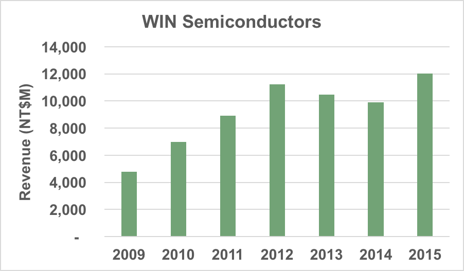
WIN has continued to provide our customers with a market advantage, and demand for our value-added solutions continues to grow. In 2015, we delivered our 1 millionth 6 in wafer. We continue to invest in our manufacturing capabilities and have recently completed refurbishment of our third factory (Fab C) that, when fully built out, will increase our total production capacity to more than 60,000 wafers per month.
WIN Semiconductors is now a publicly traded company and had its IPO in December of 2011. With our sustained business success, WIN is the single largest GaAs manufacturer worldwide, as well as the world’s 13th largest IC foundry and the 10th largest pure-play wafer manufacturer.
You serve both high volume, low cost applications, like cellular handsets, and the high mix, high performance, lower volume applications, like point-to-point radio. How are you successful executing both business models, which tend to drive opposing requirements in a fab?
One of WIN’s greatest strengths is the broad portfolio of technology solutions that enable our customers to gain share across all markets that use RF and millimeter wave components. It is quite true that these markets have diverse requirements; however, the common threads are compound semiconductor expertise and manufacturing excellence.
WIN has one of the most experienced staffs of compound semiconductor technologists in the industry, and these experts enable rapid commercialization of value-added solutions, from high-performance BiHEMT technology, for integrated Wi-Fi applications, to high efficiency HBT processes, for 4G LTE power amplifiers (PA), to the world's only commercially available 0.1 µm pHEMT platform manufactured on 6 in wafers. Our relentless manufacturing discipline drives a high degree of production commonality across all technologies and enables WIN to produce these diverse platforms in the same factory. This allows for increased operational efficiency and greater effective scale.
Additionally, our pure-play foundry model allows WIN to aggregate demand across multiple customers and market segments, which is particularly effective at increasing volume in the specialty technologies used for high performance/high reliability applications.
Discuss your GaN technology roadmap. What’s your view of market adoption?
WIN has a 0.25 µm, 28 V GaN on silicon carbide (SiC) technology (NP25) that has been in production since early 2014 and is seeing good adoption by our customers, several of which are moving to production. We continue to invest in GaN technology to address 50 V base station PAs and are presently qualifying a 0.45 µm process (NP45) and expect this technology to be released in early 2016. We also see market opportunities at higher frequencies and are actively developing a 0.15 µm process (NP15) that will address power applications through 40 GHz. This technology is in its final stage of development, and commercial release is scheduled for late 2016.
Regarding market acceptance, we see GaN technology approaching an inflection point, and adoption rates are likely to increase dramatically in the near future, particularly in the base station PA socket. Similar to the shift from bipolar devices to LDMOS for this function, we expect the transition to be driven by the need for improved efficiency and linearity performance in the higher frequency bands. Our view of this market is that GaN will quickly become the macrocell PA technology of choice over the next two to three years.
Where are you focusing your R&D and what major technological challenges are you addressing?
WIN is focusing its technology investments in areas that provide our customers with a competitive advantage in their markets. We accomplish this by continually offering advanced technologies for superior performance and value-added solutions that reduce time to market.
In the area of mobile PAs, WIN continues to offer new generations of its market leading HBT technology. This suite of optimized technologies provides higher power-added efficiency for advanced 4G applications as well as improved linearity performance, essential for meeting the requirements of 802.11ac. In addition to meeting ever increasing performance specifications, WIN is providing solutions that address the higher levels of integration needed for complex applications. These solutions are being commercialized across all platforms, from integrated BiHEMT (HBT+pHEMT) for the 802.11ac Wi-Fi market, to being the only provider of high frequency pHEMT technologies that incorporate monolithic PN diodes for compact ESD protection.
Targeting the high performance segment, we have commercialized multiple advanced integration options such as standard E/D logic cells for digital interfaces and 3+ metal layers combined with a humidity robust platform. When combined with RF isolated through-wafer via connections, these integration options provide our customers a clear path to a chip-scale package for applications through 100 GHz.
Discuss the trends you are observing in the RF semiconductor industry and how these are affecting your business.
The emerging trend we see is the accelerating transition to higher frequencies with more challenging performance specifications, both in the area of mobile devices and wireless infrastructure. These trends are driven by the continual increase in mobile data consumption and lay the groundwork for the transition to 4.5G/5G networks. These stringent performance requirements at higher frequencies align very well with the inherent advantages of compound semiconductors.
In the mobile PA space, we are starting to see performance targets at 3 GHz and above, and the move to higher frequency bands is streaming into base station PA specifications. In wireless infrastructure, the need to deliver higher peak data rates drives the deployment of point-to-point radios at E-Band and beyond. We are now seeing concerns over potential crowding at E-Band, and there is broad interest in technologies to support backhaul equipment above 100 GHz.
The impact of these trends is that WIN must be proactive and very forward looking when it comes to technology investments and adjusting our manufacturing infrastructure. We devote considerable resources to identifying the proper long-term investments to ensure WIN possesses a technology portfolio well aligned with the requirements of next generation mobile networks and user equipment.
What’s the geographic distribution of your customers and is it changing?
WIN is a key element of the compound semiconductor supply chain, and our comprehensive portfolio of production technologies places us in a unique position. Our markets and customers are remarkably diverse, ranging from very large companies that deliver billions of mobile PA products to small users who produce a few hundred ultra-high performance components for niche markets. The key point here is the compound semiconductor industry is global, and we supply customers worldwide, including all parts of the U.S., Europe and Asia.
You’re now the largest pure play, compound semiconductor foundry in the world. Where do you go from here?
To build on our record of success, WIN will continue to leverage our core competencies of compound semiconductor technology and manufacturing expertise to expand our content in existing markets as well as entirely new applications.
We see significant opportunities for our GaN platforms and intend on becoming a prime supplier to the base station PA segment. Furthermore, the evolving requirements of 4.5G/5G networks align very well with the inherent advantages of compound semiconductors. The demands for higher bandwidth and customized services means that fixed and mobile networks are becoming more complex. Inevitably, this flows down to the component level as increasingly difficult performance specifications. For the key RF, millimeter wave and optical functions, these demanding requirements can only be satisfied with compound semiconductor technology.
I am confident that our value-added technology solutions and advanced integration strategy will maximize our content in these markets and provide long-term growth for WIN.