
UMS is well known in the RF/microwave industry, yet most probably don’t know how the company was formed.
United Monolithic Semiconductors (UMS) is the result of a more than 40-year long tradition of R&D in the RF/microwaves and semiconductor domains, both in France and Germany. It was actually founded in 1996 by the combination of III-V activities from Thomson CSF (Thales) in France and DASA and TEMIC (Airbus Defense & Space) in Germany, with the objective of securing access to strategic technologies for defense and space European programs through state-of-the-art products and a foundry services offering.
Today, we are known in the industry to be addressing five main markets:
- Automotive,
- Telecoms,
- Industrial,
- Defense, and
- Space,
serving advanced applications and solutions like active antennas for defense, space or telecoms, radars for automotive or point-to-point transmission for 5G networks.
Defense and space represent around 30 percent of our revenues, as UMS developed from the very beginning and consistently over the last 24 years an innovation and growth strategy in automotive, telecoms, industrial sensors, medical and test instrumentation, reaching now 70 percent of our business.
Describe UMS’ product and service offerings and how each contributes to your revenue.
UMS offers quite a broad panel of products and services, ranging from fully open foundry access, based on our proprietary GaN and GaAs technologies, to standard or on demand products, designed on our technologies or external Si processes.
Last year, our standard product activity generated about 50 percent of our revenues, foundry services representing about 20 percent and 30 percent being related to design on demand or ASICs.
Regarding foundry services, UMS’ offer ranges from untested wafers to fully tested packaged die based on all our in-house GaAs and GaN technologies, most of which are qualified for space.
Overall, our goal is to ensure we provide, in a very flexible way, the best solutions for our customers by combining our technologies, expertise, products and packaging options with the most relevant ones on the market.
Your website describes UMS as a “European leader in offering RF MMIC products and foundry services.” Does that mean your focus is serving European needs? How much of your business is outside Europe?
Today, close to 50 percent of our business is generated outside Europe and growing as we develop our activities in North America and Asia. We are capitalizing on long-term partnerships that we have built with leading actors in their respective industries worldwide — amongst which are major European players — and on business developed with new players recognizing, in particular, our ability to adapt to their specific needs.
Although our supply chain is global, UMS’ own industrial base is in Europe, located in Germany (Ulm), where we manufacture our wafers and develop our III-V technologies, and in France (Paris area), where our products are designed, evaluated and finally tested in our back-end facilities.
We are actively participating in advanced European collaborative developments with other European key players and are at the forefront of GaAs and GaN technology development, as well as product and solution integration — all of which position us amongst European leaders for both RF MMIC products and open foundry access to our technologies.
Describe your process technologies and the capabilities of your wafer fab.
Our process portfolio includes RF GaN on SiC HEMT technologies with 0.5 to 0.15 µm gate lengths and soon 0.1 µm, together with a wide selection of GaAs technologies: low noise and power pHEMT, HBT InGaAs for VCOs, MMIC Schottky diode and MESFET processes. And we also propose a passive GaAs process for the manufacturing of high performance and low-cost filters and combiners.
UMS’ business model is based on our ability to combine this large portfolio of 15 GaN and GaAs technologies with the possibility to use external foundries for Si/SiGe technologies, to offer the solution that best fits our customers’ needs and to deliver either single or multi-chip modules in millions of high runners or very small quantities.
Consequently, our wafer fab is organized to serve that purpose and adjust dynamically to very large or only few GaN and GaAs wafer series, with no compromise on our high quality standards.
How do you package devices?
Packaging has always been a key aspect of UMS’ offering.
We were a pioneer in introducing plastic packaging for mmWave devices years ago, we then launched heterogeneous integration of different technologies inside the package and now one our key focuses is complex system-in-package (SiP) solutions, combining our internal capabilities with a strong network of research and industrial partners to go further in developing innovative and competitive solutions for all our customers.
We have built an internal assembly capability for prototyping and small quantities, a very effective service for product evaluation, test and manufacturing of demo boards expected by our clients.
And for higher quantities or large volume markets, we have developed strong partnerships with assembly partners in Asia and Europe to address, depending on the needs, from simple plastic solutions to hermetic packages for high-reliability products.
Our approach here is all about agility and efficiency.
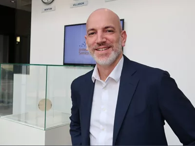
You became CEO last December. Aside from dealing with the coronavirus pandemic, what has been your focus during these nine months? Any shifts in UMS’ strategy?
Before becoming the CEO of UMS and the spread of the pandemic situation, I have been very fortunate to have the opportunity to visit, together with my predecessor, some of UMS’ key customers and suppliers, as well as industrial and institutional partners, helping me to build a good understanding of their return experience in collaborating with UMS and of their expectations for 2020 and beyond.
Since December 2019, I have increasingly met with UMS’ teams to openly discuss our key strengths and room for improvements to best serve our customers. We have also intensified the work on refining our technological, packaging and product development roadmap to best align with market needs. And we have been continuously working on further improving our operational excellence and velocity.
Our strategy is clear and focuses on technological leadership, high quality standards, increasingly integrated and packaged solutions, services to customers and constant innovation, together with our complete industrial partners network.
One of the key focuses in the next months and years will be to accelerate even more our development cycles to ensure success in our strategy execution.
How has UMS fared during the pandemic?
Happily, we were able to maintain a minimum production capacity between 50 and 60 percent and a “close to regular” functioning for all other functions throughout the peak of the crisis in Europe, thus ensuring business continuity and serving the key priorities of our customers.
The pandemic has put UMS teams’ serenity, professionalism and solidarity through a stringent test. And through their engagement, their sense of responsibility and their genuine attachment to their colleagues and to UMS, the teams collectively demonstrated that they were up to the challenge.
I am particularly proud of what UMS teams have achieved these last few months.
How does UMS maintain a competitive technology portfolio? You’re often competing with larger companies in the U.S. and Asia.
You are right, we are facing a particularly intense competitive environment in the semiconductor industry, including very large actors. UMS’ answer to that context, with regards to its processes and product catalog portfolio, is very simple: focus, innovation and agility.
In order to optimize the allocation of our resources, we made clear choices and focused on strategic and really differentiating state-of-the-art technologies and products, where we know we are competitive.
In terms of innovation, combining end-to-end capabilities — technology development, product design, foundry, back-end services — with expertise on different business models — traditional and NewSpace, defense, commercial — and partnerships with customers leading in their respective industrial domains is a clear and very stimulating advantage. We also benefit from a strong network built over the years with most European R&D labs and research centers to develop disruptive future technologies and provide support for their integration.
Regarding agility, UMS’ size is here a key asset, enabling us to react fast to customers’ demands, to have short feedback loops between technology and product development and to implement effectively all relevant adjustments and monitor performance improvements. This flexibility strongly supports innovation in engineering, acceleration of our development cycles and, in the end, fast industrialization of always more integrated solutions to our customers’ benefit.
Obviously, nothing of this would be possible without the constant full engagement of UMS’ teams. They are at the core of our competitiveness.
What are the best market opportunities for UMS during the coming five years, the opportunities driving your R&D investments?
One direction is, of course, to keep on developing our GaN state-of-the-art technologies, with a special focus on very high power-added-efficiency performance, which today pushes to reduced gate length to go up in frequency, to cover future Q/V- and E-Band needs.
Another axis is about increasing integration, that we will move one important step further. Just as an example: integration of more than ten chips is now under development at UMS together with innovative partners, enabling the design of a full SiP radio, including all RF paths with baseband, signal generation, converters, modulators and control functions.
5G MIMO, especially at mmWave frequencies, will require front-end integration in compact, low-cost and high performance solutions mixing heterogeneous devices. As an example, the European 5G-GAN2 program, led by UMS with 14 partners from eight countries, targets the development of GaN front-ends up to E-Band for 5G and other needs.
NewSpace is going to be a growing segment with higher volumes compared to traditional space business. Many companies involved are today baselining commercial-grade semiconductors and are often using industrial or automotive-grade semiconductors with an extended temperature range to provide better reliability. Consequently our high-reliability technologies and products will be a real option to be directly used by NewSpace companies.
Finally, other activities such as IoT, smart sensors and medical applications are emerging today and will certainly drive a part of our future developments and growth.
Tell us about your background and what led you to the CEO position at UMS.
Stepping back from my 21 years of professional experience, I worked for most of my career for UMS clients — Alcatel Lucent (today Nokia) and Thales — directly connected to three industry segments that UMS addresses today: telecommunications, space and defense.
Prior to joining UMS, I led an operational unit at Thales and was VP in charge of the Thales Group transformation, working in particular on product and services competitiveness with Thales businesses and on the transformation of Thales global functions. Over the years, I have held positions with Alcatel Lucent and Alstom (in the energy sector) in business development, finance, project management, business management and transformation.
What I saw in UMS, prior to joining, is a
- Unique organization with advanced technologies, products and services, serving a large variety of very demanding customers while enjoying an atypical positioning in a very dynamic semiconductor industry.
- A community of great professionals recognized by their customers, industrial partners and even competitors, always keen to embrace the next challenge and very attached to their company.
- A company facing many exciting challenges for the future, with many assets to leverage and many opportunities to embrace.
Thus, joining UMS was an obvious choice for me, and I am happy and proud to have been offered the opportunity to embark onto this fantastic collective adventure.