
I have spent countless hours and many dollars trying to eliminate impedance mismatches from transmission line interconnections, and I suspect that others may have had similar experiences. Through attempts to minimize reflections at 40+ GHz, I have come across examples where a design that meets a TDR discontinuity specification yields more reflections than one that does not.
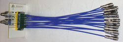
Figure 1 Multi-coaxial cable launch connector on a PCB.
My problem is exacerbated by the fact that our company’s products are multi-channel RF cable compression mount connectors and cable launch systems that mount to PCBs with hard right angles in the transmission line interfaces. Signals with 20 ps and shorter rise times do not seem to like to make sharp right angle turns. Our customers frequently tell me, “I have a ±10 percent deviation criterion on the impedance of the transmission line and if you cannot hit it, your solution will not meet our requirements.”
Through extensive research and optimization of different PCB stack-ups in order to achieve the ±10 percent target, we have learned an interesting thing: there are instances where return loss is worse for a transmission line that meets the ±10 percent specification than for a transmission line that does not. Occasionally, when designing high speed transmission lines, too much emphasis is put on meeting TDR specifications than on achieving a clean signal with fewer reflections and less transmission line insertion loss.
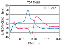
Figure 2 TDR at 20 ps resolution for a ×12 and a ×16 PCB assembly.
Our customers have an infinite number of different PCB design stack-ups that occasionally change for one reason or another, even after the design is “frozen.” It is our responsibility to use whatever tools are necessary to optimize the launches of these cable systems so our customers achieve the data rates they require, often 28 Gbps or higher. At these data rates, the signal resolution often needs to be the third harmonic of the Nyquist Frequency (for 28 Gbps, this can be 42 GHz or higher).
TDR Measurements Example
Take, for example, a PCB with a 2.92mm edge launch coaxial connector at one end of a microstrip trace followed by about a 1" trace on a PCB and a right angle transition into a cable connector (see Figure 1). Shown in Figure 2 is a TDR measurement from the edge launch to the cable for two different assemblies, each with their own PCB design but having the same connector design. TDR responses are measured using 20 ps rise time steps for a 10 to 90 percent signal level.
The two curves on this graph, one labeled ×12 and the other labeled ×16, refer to the number of total channels on the two different connectors. As the signal moves through the edge launch on the left of the graph, it encounters a slight inductive response of about 2 ohms on both curves. This inductive response is due to the mismatch on the edge launch connector. For the curve labeled ×16, the signal then goes through a PCB trace that is around 52 ohms for about 0.1 nanoseconds and then it sees a discontinuity at 0.15 ns of about 58 ohms, which is clearly outside the 45 to 55 ohm specification of many transmission line designs.
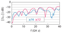
Figure 3 S11 through 40 GHz for a ×12 and a ×16 assembly.
For the curve labeled ×12, starting on the left, the signal sees the same inductive response from the edge launch but the PCB trace is much closer to 50 ohms. At 0.18 ns, the signal sees a capacitive discontinuity that corresponds to the portion of the PCB trace under the connector, effectively lowering the impedance of that portion to 47 ohms. The signal at that point sees a capture pad that is 0.018" in diameter and is the connector launch pad. The pad size is optimized to be 50 ohms with respect to the surrounding anti pad and the return layer under the microstrip trace. The return layer has a 0.040" hole in it directly under the capture pad. The signal sees the same inductive reactance at the interface part of the cable launch system (about 5 ohms) as seen for the ×16 configuration. After entering the 50 ohm coaxial cable, the impedance becomes uniform.
Time differences between the two cases are due to two factors: first the trace lengths are not exactly the same, and second, the dielectrics though they are both Megtron 6 material, are different. This highlights some of the limits of PCB and acid etch technology for extremely fast data rate applications.
S-Parameter Measurements
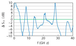
Figure 4 Differences between S11 for a ×16 and a ×12 assembly.
Looking at these two TDR curves, one might expect to see more variation in S11 for the ×16 configuration, having a higher impedance discontinuity, but this is not the case (see Figure 3). We will use S11 = -20 dB (VSWR 1.22) and S11 = -15 dB (VSWR 1.43) as reference points; S11= -20 dB since it is generally a clear transmission line with a match efficiency of 99 percent; and S11 = -15 dB because it is fairly well matched at 96.84 percent efficiency and is still, in most cases, a usable signal. The ×12 transmission line is above -20 dB at about 5 GHz and crosses the -15 dB line at 10 GHz, while the ×16 transmission line with its 58 ohm discontinuity just barely crosses the -20 dB line at 8 GHz but then dips down again and does not really go above -20 dB until above 16 GHz or so. The -15 dB point for the ×16 curve is at 22 GHz.
Figure 4 shows the differences between S11 for ×16 and ×12. On this chart, wherever the curve is above zero, S11 is lower (better) for ×12 than for ×16. ×12 is lower from 0 to 5 GHz, 7 to 9 GHz, 13 to 15 GHz, 20 to 22 GHz, and 26 to 29 GHz. If one discounts S11 measurements below -20 dB, which is a 99 percent perfect signal at 0 to 16 GHz on the ×16 S11 curve, then ×12 exhibits a lower S11 over a total of only 5 GHz of the entire spectrum to 40 GHz (20 to 22 GHz, and 26 to 29 GHz).
Insertion loss through the interfaces of both transmission lines looks very similar as both have less than 4 dB loss through 40 GHz, which includes 6" of 0.047" diameter coaxial cable attached to the interface (see Figure 5). It is important to note that the S21 curves do not start at 0,0 mostly due to the DC resistance of the transmission line, which is about 0.350 ohms. There is less than 0.2 dB of difference through most of the spectrum up to 25+ GHz. The curves start to diverge a bit more at frequencies above 25 GHz, but never by more than 0.5 dB. Note that S21 for ×12, the transmission line within the ±10 percent specification, has a noticeable dip after 38 GHz. It remains to be seen if there is a resonance after 40 GHz on the ×12 transmission line.
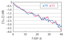
Figure 5 S21 through 40 GHz for a ×12 and a ×16 assembly.
Conclusion
TDR is a good bellwether for determining transmission line performance, but it is not the end all, as illustrated through this example. Time domain measurements are dependent on measurement variables such as rise time. In both the cases described, a rise time above 40 ps would have smoothed the TDR curves out considerably. The use of the time domain with a resolution of, in this case, 20 ps can give indications of trouble spots, but the only real way to obtain an accurate picture of a transmission line performance is to use both time domain measurements and frequency domain measurements, and measure the actual performance.
Acknowledgment
Thanks to Gert Hohenwarter from Gatewave Northern for his data and insight.