
A Digital Radio LNA
Salisbury Engineering Inc.
Salisbury, MD
The digital radio systems being deployed currently promise increases in spectrum efficiency as well as voice quality. In order to realize this performance outside the laboratory environment, the RF front ends must be more sensitive, linear and robust than their analog system counterparts. In addition, the installation techniques require operation over a large temperature and voltage range. This combination of low noise, high linearity and robustness has been realized in a low noise amplifier (LNA) designed for use in a cellular-band repeater system.
Repeaters are often deployed to extend the range of a large cell site. A block diagram for a typical cellular (or personal communications service) repeater is shown in Figure 1 . Since the repeater is filtering and amplifying a block of voice channels instead of downconverting an individual voice channel, any signals in the diplexer's pass band must be amplified by the LNA. To a large degree, the LNA's performance determines the system's performance.
 Fig. 1: A typical cellular repeater.
Three performance parameters that affect system performance the most are noise figure, linearity and dynamic range. During amplification, strong signals will mix with one another and generate intermodulation products. If the amplifier is not linear, these products will interfere with the desired signal. Typically, the figure of merit used for linearity is the third-order intercept point (IP3).
System dynamic range is determined by the difference between the minimum and maximum signal levels, which the system can process while maintaining a given signal-to-noise ratio or bit error rate. The minimum signal level that can be processed by the repeater is determined by the insertion loss of the diplexer and the noise figure of the LNA. The maximum signal level is the input amplitude that causes distortion and creates interfering signals, which mask the desired signal. The magnitude of this interference is a function of the modulation type.
RF Circuit Description
Good noise figure performance and high IP3 are not attained ordinarily with one gain stage. In the described LNA design, three gain stages are cascaded, as shown in Figure 2 , to achieve the desired 43 dB of small-signal gain.
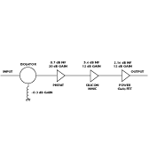 Fig. 2: The LNA block diagram.
The first stage is constructed using a pseudomorphic high electron mobility transistor (PHEMT) in a single-ended circuit. This configuration takes advantage of the low noise characteristic of the device. Due to the relatively high impedance of the noise match, a mechanism to match the transistor's input to the 50 ohm system impedance must be employed. The solution to this problem is either to balance two stages in quadrature or to add an input isolator.
The input isolator was chosen for its simplicity as the cost of both options was approximately the same. Following the production of the first lot of units, the single-ended design appeared to be both simple to tune (no phase and amplitude matching required between two balanced stages) and reproducible.
The first stage exhibits a rather narrow performance bandwidth (between four and six percent of the center frequency) caused by the relatively high impedance of this device matched by lumped element and microstrip tuning components. This narrow bandwidth is not a liability in the depicted application since the input pass band of the system is also less than four percent of the center frequency. Away from the center frequency, the gain of the overall amplifier rolls off predictably with no gain re-entry to disturb the filter response. The center frequency can be set easily at the factory during alignment and test to support nearly every cellular requirement. The input isolator exhibits > 20 dB of port-to-port isolation, providing an input impedance that is consistently predictable. This input match is important due to the LNA's location. Any mismatch loss presented to the LNA's input contributes directly to the noise figure of the system.
The IP3 of the system is critical to operation in the dense RF environments in which most systems are installed. The PHEMT transistor chosen exhibits both a low noise figure and good IP3 performance. With increasing drain current, the IP3 improves at the expense of increased noise figure. A compromise that balances these two parameters was chosen, which yields a final performance of 20 dB gain, IP3 > 23 dBm and noise figure
The second gain stage requires a different design approach than the first. The 20 dB gain of the first stage masks the noise contribution of the second stage, which relieves the need for optimum noise figure. Instead, reasonable gain and improved IP3 are required. A silicon MMIC was chosen in order to control costs while presenting the predictable input and output matches, which are critical when cascading multiple gain stages. Without this performance, undesirable gain ripple would be introduced. The final performance of the second stage across the 800 to 900 MHz band is a small-signal gain of 12 dB, IP3 > +27.5 dBm and a noise figure of 5.6 dB. The IP3 performance of this MMIC is adequate to preserve the overall LNA target specification for a minimum IP3 of +37 dBm since the final stage has an adequate IP3 margin.
The final gain stage for the LNA uses a power GaAs FET. The flanged transistor chosen is used in a broadband circuit with negative feedback. The negative feedback enhances stability, improves the input match to the preceding stage and reduces third-order intermodulation products. These improvements come at the cost of a reduction in output power at the 1 dB compression point (P1dB) and gain performance. The final stage's performance was measured at a gain of 12 dB, noise figure +39.5 dBm. When cascaded with the other two stages, the final lineup proved to be stable with high output power. When the LNA is driven to compression, nearly 1 W of output power is available. Figures 3 and 4 show the overall LNA performance.
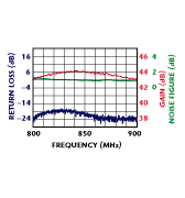 Fig. 3: LNA measured performance.
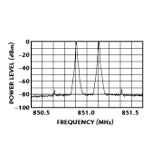
Fig. 4: Two-tone intermodulation distortion.
Power Supply Design
With the RF lineup established firmly, the power supply design was approached to address the hostile environment of a remote site installation. The supplied DC voltage can vary from 18 to 32 V DC. Due to the wide variation in input voltage, a bucking regulator was designed to incorporate both reverse- and over-voltage protection. The regulator's input and output lines are filtered and regulated to prevent the introduction of spurious products into the system. Special circuitry provides gate sequencing to prevent destruction of the final gain stage's power FET. The LNA's total current consumption is nominally 300 mA at 24 V DC.
Cooling
Although the LNA consumes 7.2 W, no special cooling is required for most applications. The bucking regulator levels heat generation over the supply voltage range. A heat sink is incorporated into the cover. The baseplate is flat and unpainted to allow for further heat sinking if desired.
Conclusion
Although the performance of the LNA in the laboratory has exceeded all of the design goals, the true test of the design is in the field. If the band-limiting system components that precede and follow the LNA are not chosen properly, the full benefit of the LNA's performance will not be realized. Drawing upon many years of diplexer and filter experience, an integrated assembly was constructed, which reduced the risk of poor field performance.
A solution to many of the problems associated with the harsh RF environment encountered in the field is now available. The final LNA design performs well without the use of exotic technologies, thereby providing a cost-effective and high performance system solution.
Salisbury Engineering Inc.,
Salisbury, MD (800) 989-2141 or (410) 543-2141.