
This article describes an innovative education kit known as Eductika. It is dedicated to students and teachers in electronics. The main concept is the assembly of basic puzzle elements to create microwave passive components such as filters, couplers and antennas. The design of an ultrawideband filter using this kit is provided as an example. All steps from theory through measurement are illustrated. Good agreement is shown between the simulation and the measurement.
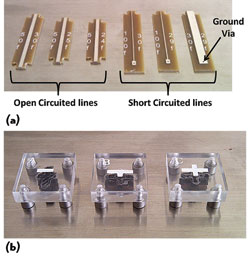
Figure 1 Microstrip Lines (a), Connecting Items (b): Direct Connection [A], T-Junction [B], Cross junction [C].
The development of new applications in telecommunications has contributed to the rapid increase of wireless technology, especially within the microwave electronics field. The field of microwave electronics requires good theoretical and practical knowledge of waveguide propagation, lumped/distributed element concepts and wavelength related phenomena, as well as knowledge of electromagnetic (EM) simulation techniques such as 2D planar and 3D full-wave.1-3 This is why Elliptika has developed an education kit known as Eductika.4 The scope of this first education kit is microstrip passive devices but other applications, such as antennas, are also under development. Eductika allows one to build partial or entire passive microwave functions from basic puzzle elements.
Eductika is composed of basic sub-sets of microwave passive components aimed at teaching students microwave fundamentals. It offers a simple way to acquire, through practice, skills in various subjects such as the physics of microstrip lines, impedance matching devices and synthesis of elementary functions (e.g., couplers, power dividers, bandpass/lowpass filters, short/open circuit stub filters) as well as some passive functions of higher complexity based on these elementary functions.5 Furthermore, Eductika helps students to become familiar with the use of measurement instruments such as the vector network analyzer (VNA).6 This education kit also allows students to use computer aided design (CAD) tools. In fact, there is collaboration between Elliptika and ANSYS®7 to improve the simulation part of the kit. This partnership has led ANSYS to create a new library in its simulation tool, ANSYS DesignerRF™, in which it incorporates the puzzle pieces of microwave components proposed by Eductika. This enables students to verify theory through simulation before implementing and testing their microwave designs.
In this article, we discuss the principle of the microwave puzzle with a description of the various puzzle pieces found in the Eductika kit and the resources available in the ANSYS high frequency toolkit library. As an example, to demonstrate how the kit may be used, we describe the steps for the design and construction of an ultra wide bandpass (UWB) filter based on short circuited stubs.
Eductika components puzzle
This very complete puzzle game consists of microstrip line sections with different impedances and lengths which can be seen printed on the pieces. These lines can simply be linked together by different connecting items (e.g., T-junction, cross junction or a direct connection between two lines). Figure 1a and Figure 1b show puzzle pieces with examples of open and short circuited lines and connections. Figure 2 shows a set of components from the Eductika library (a) not connected or (b) interconnected in order to build a microwave circuit. The connecting items positioned between the microstrip puzzle pieces ensure an electrical contact between the metal tracks of adjacent puzzle pieces on a magnetic plate.
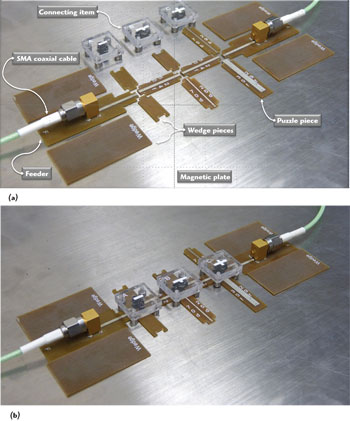
Figure 2 A set of components from Eductika library (a), Components interconnected to build a microwave circuit (b).
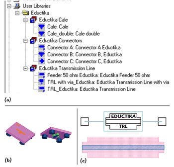
Figure 3 Eductika library in ANSYS DesignerRF™ (a), 3D view of connector B, (b) Symbol and footprint of microstrip line (c).
To help students understand electromagnetic field, circuit and system simulation software, ANSYS has developed, in partnership with Elliptika, an Eductika toolkit library for ANSYS DesignerRF. This library, Figure 3a, includes the basic elements of the Eductika kit: microstrip lines open or short circuited, connectors and feeds.
The microstrip lines are parameterized in width and length, enabling the user to reproduce all elements of the physical Eductika kit. Each element of the library, Figure 3b, consists of a symbol and footprint associated with an analytical model – Figure 3c. The student starts a design by selecting the Eductika technology file, which automatically loads the library, substrate and stackup definition. The student builds the microwave function by connecting the components in the schematic. This automatically creates the layout the same way as the circuit is assembled on the magnetic plate with Eductika Kit (see Figure 4). Using the ANSYS DesignerRF Solver On Demand (SOD) technology, the student is able to run, in just a few clicks, a simulation with different solvers: Circuit (Nexxim), 2.5 EM (Planar EM) and 3D EM (HFSS). The Eductika toolkit library for ANSYS DesignerRF is provided with eight tutorials that guide the student to build and simulate different microwave functions in ANSYS DesignerRF.
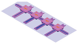
Figure 4 3D view of the UWB filter in ANSYS Designer.
Theory of a 4th order UWB filter
The “Bandpass stub filters” box provides a way of studying the design of broadband bandpass filters with stubs in microstrip technology.4 The filter is designed on Neltec substrate with relative permittivity of 3.8, loss tangent of 0.007, and thickness of 0.711 mm. The trace metal is copper with a metallization thickness of 17 µm. This practical class activity has three parts: design, synthesis and simulation. The filter is required to have a center frequency of 1.5 GHz with a bandwidth (BW) of 750 MHz. Figure 5 shows a schematic of the proposed 4th-order UWB filter achieved using ideal lines. It consists of four λ0/4 short-circuited (SC) stubs placed in parallel and interconnected by three quarter-wavelength admittance inverters.4 The wavelength in the propagation medium is λ0 at the center frequency (f0) of the filter. In Figure 5, Z0 designates the input and output impedances of the filter. Z1, Z2, Z3 and Z4 are the characteristic impedances of the four short-circuited stubs and Z12, Z23 and Z34 are the characteristic impedances of the three interconnecting lines.
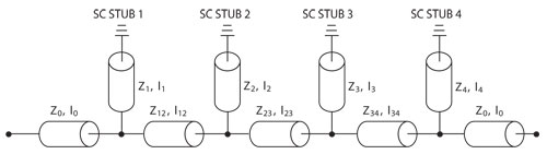
Figure 5 Fourth order UWB filter.
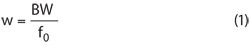
To design the filter, the Tchebyscheff approximation is used with a bandwidth ripple Am 50.01 dB. After specifying the relative bandwidth (w) by
the characteristic impedances of the SC stubs and the interconnection lines are calculated using equations 1 to 10 in Reference 1 (p. 57). With Z0 5 50 Ω, and for d 5 0.9 (where d is an adjustment parameter of the filter), the values of Z1, Z2, Z3, Z4, Z12, Z23 and Z34 are:
Z1 = Z4 550.0 Ω
Z2 = Z3 530.1 Ω
Z12 = Z34 548.4 Ω
Z23 = 49.1 Ω
Simulation and Measurement
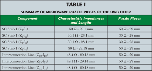
Once the theoretical study is completed, the high frequency toolkit of ANSYS DesignerRF is used to verify the electrical response of the UWB filter. As mentioned, the collaboration of Elliptika and ANSYS has led ANSYS to create a library that contains puzzle pieces of the Eductika kit. The filter is simulated by using microstrip puzzle pieces and realized on a Neltec substrate (εr 53.8, h 50.711 mm). The company uses the microstrip line calculator of ANSYS DesignerRFto determine the different lengths of puzzle pieces. Table 1 summarizes the characteristic impedances and lengths of the UWB filter and the corresponding puzzle pieces that can be found in the Eductika kit.
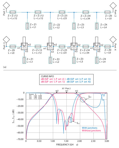
Figure 6 Schematic circuit of the UWB filter with junctions (bottom) and without junctions (top) (a), and associated electrical responses (b).
Figure 6a shows the schematic circuit of the UWB filter realized by ANSYS DesignerRF software with and without taking into account the junctions between the lines. The associated electrical responses are presented in Figure 6b. The comparison between responses shows a difference at high frequencies. The electrical response of the circuit without junctions is what is desired; however, when junctions are added, undesired capacitive effects influence the electrical response at high frequencies. To adjust the response, one option is to modify the length of the interconnecting transmission lines. The new values are shown in Table 2. Figure 7 shows the electrical response of the modified UWB filter which now corresponds to the desired response.
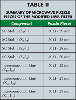
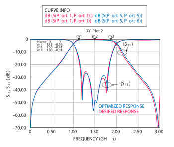
Figure 7 Desired filter response (red line) compared with the response of the optimized design (blue line).
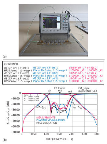
Figure 8 Network analyzer display showing the response of the assembled UWB filter (a), circuit simulation of the modified UWB filter design (black line) compared with the measured response of the assembled filter (red line) (b).
Once theoretical design and the simulation are complete, the UWB filter is built on a magnetic plate, Figure 8a, and measured using an Anritsu VNA. Figure 8b compares measurement and EM simulations, showing good agreement, particularly in terms of passband insertion loss and stopband rejection. Insertion loss at the center frequency, for example, is 1.31 and 1.25 dB, respectively, for HFSS simulation versus measurement. Moreover, the desired bandwidth of 750 MHz was achieved.
Conclusion
Eductika provides students with a comprehensive understanding of high frequency circuits, from theory through measurement. Using a puzzle game, students can readily construct circuits using different passive microwave components. It enables students, through a structured and interactive learning environment, to become familiar with complex electromagnetic concepts and tools used for design, simulation, and measurement.
References
- J. Hong and M.J. Lancaster, Microstrip Filters for RF/Microwave Applications, John Wiley & Sons Inc., July 2001.
- I.C. Hunter, Theory and Design of Microwave Filters, IEE, UK, 2001.
- N. Marcuvitz, Waveguide HandBook, Peter Peregrinus Ltd. UK, 1986.
- G.L. Matthaei, L. Young and E.M.T. Jones, Microwave Filters, Impedance-Matching, Networks, and Coupling Structures, Artech House, Norwood, MA, 1980.
- www.eductika.com
- www.anritsu.com
- www.ansys.com