
The printed circuit board area inside of a smartphone has become the second most precious—and contested—real estate in the mobile landscape, right behind radio spectrum. Ironically, the proliferation of newly-added radio spectrum bands—aimed at alleviating bandwidth scarcity—is what has intensified the pressure on PCB space in smartphones. More bands demand more discrete RF front-end components such as power amplifiers, multiband switches, duplexers and filters, along with matching components. Add the demands for bigger screens, quad-core application processors, connectivity, batteries and add-ons, all wrapped up in thin sleek form factors, and it is clear there is no room to expand the space devoted to RF front-ends, even to accommodate the doubling or tripling of bands needed for global LTE roaming in a single-SKU design (see Figure 1).
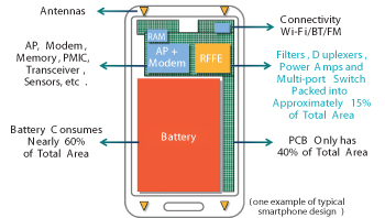
Figure 1 Limited PCB space in a typical smartphone.
The Qualcomm® RF360 RF front-end solution from Qualcomm Technologies Inc. (QTI) has been designed to address this issue, and others, with a highly integrated RF front-end combining essentially all the components between the modem and the antenna: an RF power amplifier integrated with the antenna switch, the transceiver, an antenna matching tuner and an envelope power tracker. This is a “360-degree” approach to simplifying and addressing multiple complex challenges to the cellular RF front-end, starting with band proliferation and extending across multiple performance and size enhancements so product appeal—as well as the significant production scale advantages of reducing unique SKU designs—can be maximized. Announced in February for OEM products anticipated to ship later in 2013, the front-end has been designed from the ground up as a full system solution that also works interactively with the device’s modem, transceivers and sensors to deliver unique new performance gains.
Design Approach
At the broadest technological level, the design primarily addresses the RF band fragmentation that comes with the expansion of 4G LTE (FDD and TDD) on top of continuing 2G and 3G coverage worldwide, and the need to support all the associated bands in a single device, or at least fewer SKUs and to do that without increasing the demand for space or compromising performance.
At an economic level, it is also designed to enable production scale—and its dramatic cost benefits—for cellular device manufacturers. Instead of needing up to ten different designs to competitively support the required LTE band combinations around the world, an OEM may only need three, or even fewer, and the differences across those can be addressed without a change in board layout, or an increase in board space.
RF Band Proliferation With No Increase in PCB Space
The central RF challenge today is the proliferation of cellular bands worldwide—already 40 and counting—required to address exploding service demands and network capacity. This is compounded by the need to simultaneously launch multiple handsets to meet OEMs’ desire to maximize their returns on product investments. This has pushed mobile device makers to develop multiple versions of each device model, each with smaller production unit potential, using legacy RF solutions that handle only a subset of bands or require multiple chipsets in a single device for greater regional coverage.
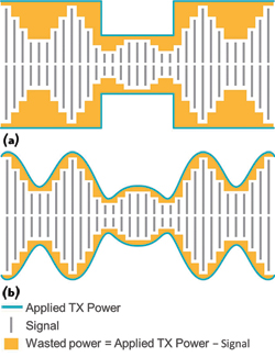
Figure 2 Power wasted with average power tracking (a) compared to power saved with power envelope tracking (b).
The Qualcomm solution addresses this RF band proliferation challenge with a single board-level SKU designed to work across any combination of modes and bands (all major cellular modes from GSM onwards and bands currently fully specified in 3GPP) that enables global roaming, particularly for 4G LTE. How is this possible, when no single RF solution can yet address all bands worldwide, without resorting to a brute force approach using a large number of discrete parts? It actually requires a combination of key technologies, all of which are integrated into the Qualcomm solution and optimized as an end-to-end system.
Power Envelope Tracking
The first key technology is power envelope tracking (ET) that tailors the PA power supply to the instantaneous needs of the signal content being transmitted. It is an advancement over conventional average power tracking (APT), that adjusts the PA power supply on power level groupings instead of on the instantaneous signal need. The unused energy with APT not only wastes battery power, but also generates waste heat, creating added demands for space for dissipation of the heat (see Figure 2a). With envelope tracking, the transmission power supplied is tailored to the instantaneous needs of the signal content being transmitted (see Figure 2b).
Working interactively with the device’s modem, the envelope power tracker adjusts transmission power to match instantaneous requirements of the content being transmitted, rather than adjusting after long intervals of constant power. This modem-assisted envelope tracking, the first in the industry for 3G/4G LTE, reduces power consumption by up to 20 percent, and heat generation by almost 30 percent (based on QTI testing and analysis). This extends battery life and reduces the thermal footprint inside the thin cavity of a smartphone.
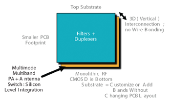
Figure 3 RF POP 3D design CMOS front-end.
Envelope tracking works with the modem to sense instantaneous power needs, and manages the PA. With CMOS-based PAs, the level of integration can be substantially increased, and points toward the idea of a fully integrated RF front-end system-on-chip. A system-on-chip means advanced 3D packaging techniques have now become possible for the RF front-end.
RF POP
The second key technology in the Qualcomm front-end solution is the industry’s first stacked, 3D RF packaging, or RF POPTM solution, using advanced 3D packaging that integrates the single-chip multimode power amplifier and antenna switch (AS) into a base package, integrates the filters and duplexers onto a single substrate and then stacks the substrate on top of the base package into a single “3D” chipset combination, reducing overall complexity and eliminating the need for the wire bonding commonly used in today’s RF front-end modules. The package containing the integrated PA and AS form the base substrate layer, and have a common footprint for all devices. The package containing the filters and duplexers is configurable for global and/or multi-regional band combinations and goes on top of the PA/AS base, much like a customizable “roof” over a universal foundation. The combination is one millimeter thick and uses half the board area of previous Qualcomm RF front-end solutions. Importantly, customizing devices for different regions does not require changes to the board layout since the base PA/AS layer can remain constant (see Figure 3).
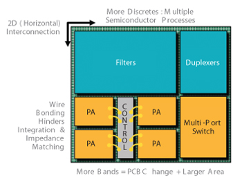
Figure 4 Side-by-side conventional RF front-end discrete design.
This design is based on an architecture capable of supporting 700 MHz to 2.7 GHz LTE bands worldwide, along with legacy 2G/3G bands, and reduces local RF band customization to simplified variations in the “roof.” With the RF POP approach, two to three PCB designs can now replace what would take a dozen or more designs otherwise to cover an OEM’s worldwide needs, since multiple frequency configurations can use the same board layout. This creates the potential to drive LTE economies of production scale in much the same way that quad-band did for GSM and penta-band did for 3G.
In contrast, conventional PCB module-based solutions mix and match different technologies such as GaAs- and CMOS-based components device-by-device for an optimum solution within a single device’s operating environment. Accommodating a broader array of environments is more complex, resulting in some cases in multiple solutions residing side-by-side within a single device. These side-by-side solutions require multiple PAs, depending on the band combinations being designed for, with more discrete chips and the associated wire bonding, which hinders integration due to introducing radiated interference and added impedance matching requirements. If more bands are needed, a board change is required, including the possibility of a size increase, and reducing the volume potential of each unique design (see Figure 4).
Adaptive Antenna Tuning
The third key technology is adaptive antenna tuning. One RF problem that has been exacerbated by thinner, sleeker device designs is that the much closer physical proximity of users’ hands and head to the antenna causes the antenna to de-tune from the targeted frequency, losing signal with the base station beyond the signal attenuation caused by the physical impediment of the hand and/or head. The base station responds by instructing the device to increase transmission power to compensate for the lost signal. If more device transmission power is available, battery drain is increased. If the device is already at maximum transmission power, the call is compromised or dropped (see Figure 5).
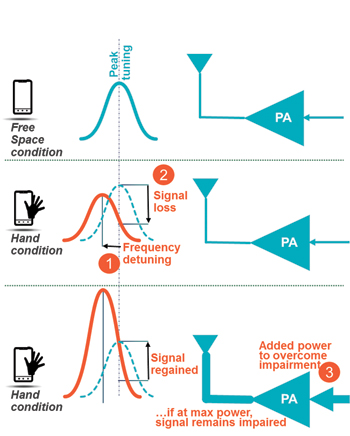
Figure 5 Conventional RF front-end de-tuning causes power increase or call drop.
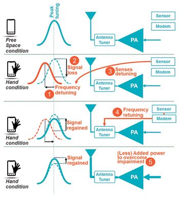
Figure 6 Qualcomm RF 360 de-tuning provokes re-tuning.
In contrast, the Qualcomm system works with the device’s sensors, which detect the antenna de-tuning and gain loss, and the modem directs the antenna matching tuner to re-tune to the correct frequency. This eliminates the need to increase power to compensate for off-frequency transmission, reducing the power increase to only that needed to compensate for the attenuation caused by the physical impediment (see Figure 6).
Power Amplifier Performance
The Qualcomm RF360 solution utilizes a comprehensive system design to enable an all-CMOS RF front-end, which historically has been judged inadequate to meet cellular power performance requirements, when compared to the module-based, GaAs/CMOS mixed technology approach. However, testing by QTI has demonstrated that—utilizing only the current generation power envelope tracking enabled by the CMOS integration—transmission power performance (power consumption for TX power produced) of the Qualcomm solution closely matches the profile of conventional power amplifiers using today’s average power tracking across the broad range of transmission power levels (see Figure 7).
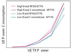
Figure 7 PA performance comparisons.
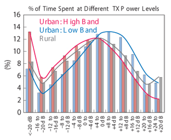
Figure 8 TX power usage patterns.
The Qualcomm solution with envelope tracking and the conventional average power tracking solution have small differences at different power levels. The system has been optimized for performance efficiency to deliver best in class talk time and data transmission across power ranges most used in real world experience (see Figure 8), based on QTI field data collected across commercial networks in rural California from 8 AM to 8 PM over seven days in 2013 and urban Los Angeles from 6 AM to 7 PM over one day in 2011, and closely matches the profile of conventional power amplifiers even outside of these most used ranges of transmission power.
When power performance is weighted based on real-world usage distribution patterns across high and low bands, the total power consumption using the Qualcomm RF360 solution is virtually identical to conventional PAs for rural settings and slightly better for urban settings (see Figure 9).
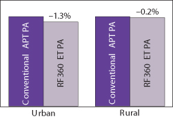
Figure 9 Usage-based total power consumption comparisons.
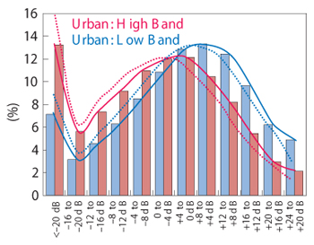
Figure 10 Shift in TX power usage patterns with antenna tuning.
It is worth noting that these performance comparisons do not factor in improvements from the use of precision analog circuitry to optimize PA and ET operation, for example, through the addition of multiple programmable gain states. Antenna tuning gains have also not been factored into the comparison. QTI Testing has shown a 2 dB gain contribution from antenna tuning, which would shift the frequency of TX power usage curves “left” by –2 dB in the usage patterns (see Figure 10).
Applying these shifted TX power usage frequency distribution patterns to the performance analysis would indicate additional improvements in total power consumption. So even without PA optimizations and antenna tuning gains, overall system performance meets today’s requirements and is comparable in efficiency to existing front-end solutions, accomplished with a much smaller PCB space requirement and much greater RF band scalability.
Conclusion
The Qualcomm front-end is a collection of innovations:
- The first fully integrated monolithic die multimode, multiband CMOS power amplifier with an integrated antenna switch
- The first stacked RF POP solution (3D packaging) that reduces the RF front-end footprint while enabling common board layout and simplified RF band customization or expansion
- The first CMOS power amplifier for LTE
- The first CMOS power amplifier with envelope tracking
- The first dynamic reconfigurable LTE multimode antenna tuner
- In total, the first fully integrated CMOS-based RF front-end, including everything between the modem and the antenna
The solution is focused on addressing the fact that worldwide LTE band proliferation has created a direct challenge to producing mobile devices at economic scale, and doing it within an extremely limited PCB space. The RF POP approach enables a common global board-level design, with simplified RF band expansion or customization, to help regain device design and production scale. Smaller RF front-end footprint, heat dissipation and size, along with longer battery life, help enable sleek, thin, powerful and efficient device designs. Plus, the solution is sampling now in order to meet the immediate challenges of establishing LTE economies of scale and global roaming.