
A Ku-Band push-push voltage-controlled oscillator (VCO) based on a substrate integrated waveguide (SIW) resonator is presented. The push-push oscillator configuration is chosen to realize a fundamental oscillator and a frequency doubler in one circuit. A varactor-loaded SIW resonator is designed to achieve electrical tunability. In order to ensure accuracy and reliability, all the designs are simulated with a full electromagnetic (EM) wave simulator. As the experimental results show, the range of the output frequency is from 13.98 to 14.09 GHz, with a frequency tuning range of 110 MHz. The output power is –1.85 dBm, while the suppression of fundamental frequency and the third harmonic are –15.37 dBc and –23.80 dBc, respectively, and the phase noise is –101.27 dBc/Hz.
Recently, with the increase of the operating frequency in modern communication systems, the requirements for the local oscillator (LO) have become more strict. Therefore, the study of microwave and millimeter wave oscillators have become more popular. But since there is a limit to the available frequencies of active devices, new methods are needed to increase the operating frequency. The push-push configuration provides an acceptable approach to solve this problem.1
In addition to the operating frequency, the phase noise of an oscillator is also a critical performance parameter. In theory, as the frequency increases, the phase noise becomes worse. So in the high-frequency oscillator design, a high-Q resonator is used to reduce the phase noise. In practice, a voltage-controlled dielectric resonator oscillator (DRO) is widely used in microwave bands.2 The high performance of a DRO is mainly due to the use of a high-Q dielectric resonator. However, the defects of traditional DROs are also obvious. As the external working environment changes, the dielectric resonator may fall off the surface of the substrate. Then, the system cannot work reliably. In addition, the volume of a DRO is sometimes not acceptable in some uses.
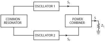
Figure 1 Push-push oscillator schematic.
The substrate integrated waveguide (SIW) is a new transmission structure proposed in recent years.3 The components based on SIW technology not only have the advantages of high-Q value, low insertion loss and low cost, but also can be integrated easily with other planar circuits.4,5 So a resonator based on SIW technology is suitable for the design of a highly reliable planar VCO. A Ku-Band push-push VCO based on a SIW resonator is investigated theoretically and experimentally in this article.
Theory
The general configuration of a push-push oscillator is composed of a common resonator, a power combiner and two identical fundamental oscillators, as shown in Figure 1. Here, S1 and S2 are the signals generated by the two identical oscillators.
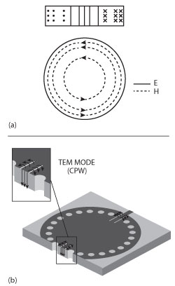
Figure 2 The cylindrical SIW resonator (a) E-field distribution of TM010 and (b) SIW-CPW transition.
S is the signal combined by S1 and S2. The basic theory of push-push oscillator is to cancel out the odd harmonic frequencies and enhance the even harmonic frequencies.6 It means that the push-push oscillator can realize the functions of the oscillator and frequency doubler. In other words, the second harmonic frequency is the output frequency. In order to reach this function, the signals generated by two identical oscillators should be out of phase at the fundamental frequency. The process can be expressed as follows:6
These two signals are identical in frequency and amplitude, but a phase difference ω0∆t is added on signal S2. With a phase difference of π, the output signal S = S1 + S2 can be expressed by:
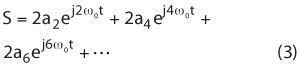
As Equation 3 shows, the odd harmonic frequencies (ω0, 3ω0, 5ω0, …) of combined signal S are suppressed, while the even harmonic frequencies (2ω0, 4ω0, 6ω0, …) are enhanced.
Design Approach
The Varactor-Loaded SIW Resonator
The dominant mode of a cylindrical SIW resonator is TM010, and the high-order mode is TM110.7 The electromagnetic field distribution of TM010 and the transition of SIW-CPW8 are shown in Figure 2. Because the resonance frequency of TM110 is much higher than TM010 and the coupling of TM110 by the SIW-CPW transition is so weak, there is no need to care about the high-order mode in the resonator. By analyzing the field distributions of TM010 and of the SIW-CPW transition, it is obvious that the induced currents in the two coupling microstrips are in-phase. According to the theory of push-push oscillator, the common cylindrical SIW resonator should be designed at the fundamental frequency. Since the field distribution of SIW is similar to that in a traditional metallic waveguide, the dimensions of cylindrical SIW resonator can be calculated by Equation 47 and the empirical Equation 5:9
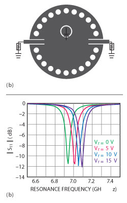
Figure 3 Simulation of the varactor loaded SIW resonator (a) and simulated S11 results (b).
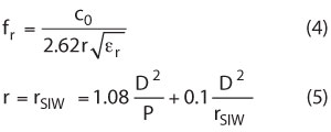
where fr is the resonance frequency, c0 is the velocity of light in free space, εr is the permittivity of substrate, r is the radius of corresponding metallic waveguide cavity, rsiw is the radius of the cylindrical SIW resonator, D is the diameter of the metallic via holes and P is the distance between two vias.
In order to achieve the electrical tunability, a varactor should be added properly into the resonator. But since the SIW top and bottom surfaces are connected by the metallic via holes, the varactor cannot be added directly to the surface of SIW. Therefore, if a circle is etched on the surface, then the bias of the varactor can be achieved. Furthermore, the circle can realize the coupling between the varactor and resonator.10
The EM simulation model of varactor-loaded SIW resonator and the simulated results are shown in Figure 3. The varactor model is replaced by an ideal tunable capacitance. The selection of the capacitance value is based on the datasheet of the varactor SMV1233 (Skyworks). The simulated resonance frequency of the varactor-loaded SIW resonator is from 6.94 to 7.09 GHz, with a tuning range of 150 MHz.
The Anti-Phase 3 dB Wilkinson Combiner
When designing a push-push oscillator, the most important point is to ensure that the two oscillators are strictly symmetrical and independent. So the isolation of two oscillators is critical. According to the analysis of the SIW resonator, the signals generated by two identical fundamental oscillators will be in-phase, which is due to the in-phase induced currents. So a 180° phase shift delay line should be added to one branch of the power combiner. This is the difference with the traditional push-push oscillator.
The configuration of an anti-phase 3 dB Wilkinson combiner and the simulated results are shown in Figures 4 and 5, respectively. Additionally, a first-order coupled-line filter is designed to block the DC. Furthermore, the filter can transmit the second harmonic frequency to the output port as a high-Q coupling capacitance. The line length is a quarter-wavelength at the second harmonic frequency. As Figure 5 shows, two signals are anti-phase at 7 GHz and in-phase at 14 GHz, after using the 180° phase shifter. Furthermore, the isolation of the two signals is above 30 dB and the return loss is above 20 dB at the input and output ports.
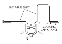
Figure 4 Configuration of an anti-phase 3 dB Wilkinson combiner.
The Negative Resistance Oscillator
In the microwave band, there are two types of oscillators: the series feedback and parallel feedback.7 The oscillators used in a push-push oscillator are the series feedback type and the design method is based on the theory of a negative resistance oscillator.11
According to the theory of the series feedback oscillator, a microstrip open-circuited stub, added to the source of the FET, can achieve negative resistance characteristics by tuning the length of the stub until the reflection coefficient Gin is greater than 1 at the fundamental frequency, as seen from the gate of the FET. It means the transistor is unstable at the desired frequency.
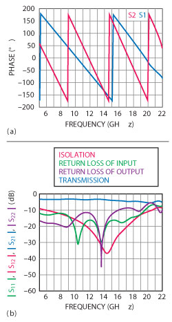
Figure 5 Simulated results of (a) phase and (b) amplitude.
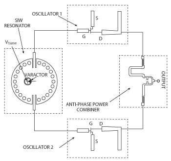
Figure 6 SIW push-push VCO configuration.
In order to suppress the fundamental frequency, the output matching network is matched at the second harmonic. As a result, the isolation of two oscillators at fundamental frequency can be enhanced. Then the frequency offset of one oscillator, due to the interference of the other oscillator, can be minimized. At the output port of the matching network, a λ/4 open-circuited stub is added to achieve further suppression at the fundamental frequency (λ is the wavelength at the fundamental frequency).
The configuration of the proposed SIW push-push VCO is shown in Figure 6. It is composed of a varator-loaded SIW resonator, two identical fundamental oscillators and an anti-phase power combiner. The simulation of the oscillator is done with an EM simulator.12 Through the connection between the schematic and layout simulator, the model of the layout can be added to the schematic, a process which ensures the accuracy and reliability of the design. The EM simulation of the SIW push-push VCO is shown in Figure 7.
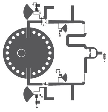
Figure 7 Co-simulation in the EM simulator.
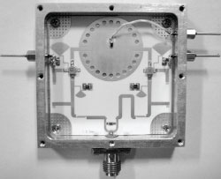
Figure 8 Photograph of the SIW push-push VCO.
Experimental Results
The circuit was fabricated on a Rogers 4350 substrate, with a dielectric constant εr = 3.66, and a thickness = 20 mil. A photograph of the SIW push-push VCO is shown in Figure 8. The GaAs FET is a MGF1801 (Mitsubishi), whose maximum available frequency is 12 GHz. The VCO is measured using a spectrum analyzer (R&S FSP40), with a phase noise measurement function. The measured performance parameters include the output frequency, the output power, the phase noise, the fundamental frequency and third harmonic frequency suppression, as well as the tuning range. The operating voltage and current of each FET are 3 V and 55 mA, respectively.
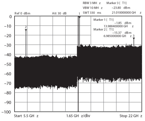
Figure 9 Measured spectrum when Vr = 0 V.
As shown in Figure 9, the output frequency is 13.98 GHz and the output power is –1.85 dBm (Vr = 0 V). The fundamental frequency and third harmonic frequency suppression are –15.37 dBc and –23.80 dBc, respectively. Also, the output frequency of the VCO is from 13.98 to 14.09 GHz, with a frequency tuning range of 110 MHz, which is enough for application in a phase-locked loop (PLL) single point frequency source. Figure 10 shows the measured phase noise spectrum when Vr = 0 V. The SSB phase noise can achieve –101.27 dBc/Hz.
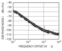
Figure 10 Measured SSB phase noise spectrum.
Conclusion
A SIW push-push VCO is designed and fabricated. By using the resonator based on SIW technology, the proposed push-push VCO reaches the goal of low phase noise. The tuning range is also enough for a single point PLL synthesizer, where a DRO is usually used. The reliability of the proposed VCO is higher and the volume lower than a traditional DRO. The proposed VCO, based on SIW technology, can be designed and simulated in an EM simulator. It ensures the accuracy of design and decreases the time of test. Because of its advantage of breaking through the available frequency of active devices, the push-push VCO provides a promising approach for the oscillators in microwave and millimeter waves.
References
- F.X. Sinnesbichler, “Hybrid Millimeter-Wave Push-Push Oscillators Using Silicon-germanium HBTs,” IEEE Transactions on Microwave Theory and Techniques, Vol. 51, No. 2, February 2006, pp. 422-430.
- O. Ishihara, T. Mori, H. Sawano and M. Nakatani, “A Highly Stabilized GaAs FET Oscillator Using a Dielectric Resonator Feedback Circuit in 9-14 GHz,” IEEE Transactions on Microwave Theory and Techniques, Vol. 28, No. 8, August 1980, pp. 817–824.
- D. Deslandes and K. Wu, “Single-Substrate Integration Technique of Planar Circuits and Waveguide Filters,” IEEE Transactions on Microwave Theory and Techniques, Vol. 51, No. 2, February 2003, pp. 593-596.
- S. Lin, S. Yang, A.E. Fathy and A. Elsherbini, “Development of a Novel UWB Vivaldi Antenna Array Using SIW Technology,” Progress In Electromagnetics Research, Vol. 90, 2009, pp. 369-384.
- W. Shen, W.Y. Yin, X.W. Sun and J.F. Mao, “Compact Coplanar Waveguide-Incorporated Substrate Integrated Waveguide (SIW) Filter,” Journal of Electromagnetic Waves and Applications, Vol. 24, No. 7, 2010, pp. 871–879.
- J.F. Gravel and J.S. Wight, “On the Conception and Analysis of a 12-GHz Push-Push Phase-Locked DRO,” IEEE Transactions on Microwave Theory and Techniques, Vol. 54, No. 1, January 2006, pp. 153–159.
- D. Pozar, Microwave Engineering, 3rd Ed., Wiley & Sons, New York, NY, 2004.
- A. Patrovsky and K. Wu, “Coupling Mechanism in Hybrid SIW-CPW Forward Couplers for Millimeter-Wave Substrate Integrated Circuits,” IEEE Transactions on Microwave Theory and Techniques, Vol. 56, No. 11, November 2008, pp. 2594-2601.
- F. Xu and K. Wu, “Guided-wave and Leakage Characteristics of Substrate Integrated Waveguide,” IEEE Transactions on Microwave Theory and Techniques, Vol. 53, No. 1, January 2005, pp. 66–73.
- F.F. He, X.P. Chen, K. Wu and W. Hong, “Electrically Tunable Substrate Integrated Waveguide Reflective Cavity Resonator,” 2009 Asia Pacific Microwave Conference Digest, pp.119–122.
- K. Kurokawa, “Some Basic Characteristics of Broadband Negative Resistance Oscillator Circuits,” Bell System Technical Journal, Vol. 48, No. 6, July-August 1969, pp. 1937-1955.
- F. Ramirez, J. Garcia, T. Fernandez and A. Suarez, “Nonlinear Simulation Techniques for the Optimized Design of Push-Push Oscillators,” 2003 IEEE MTT-S International Microwave Symposium Digest, pp. 2157-2160