
A single chip transceiver for ultra-wideband (UWB) impulse radio is described in this article. The UWB transmitter implements a low power Gaussian shaping filter to reduce the side lobes in the frequency domain, and a simple pulse amplitude modulation (PAM) is employed to maintain the low power consumption. The proposed architecture features a simple design, low-power operation and enables the pulse-shape generation for a multi-channel UWB radio. A low power UWB receiver was implemented with a pulse detector for the demodulation. This receiver is for the three lower bands of the UWB from 3.1 to 5 GHz. The IC is implemented using a 0.18 µm RF CMOS technology with a 1.8 V power supply. The total current consumption of the transceiver is 17 mA.
Impulse radio ultra-wideband communication (IR-UWB), using impulse signals that have an ultra wide bandwidth, is a specific form of UWB where the data bits modulate the short pulses in the time domain. An IR-UWB transmitter must comply with Federal Communications Commission (FCC) regulations.1 To avoid interference with the wireless local area network (WLAN) band at 5 GHz, the UWB transmitters often operate in either the
3 to 5 GHz band or the 6 to 10 GHz band. In the selected 3 to 5 GHz band of this transceiver, the bandwidth of the impulse signals is restricted to a few hundred megahertz for the multi-channel operation. The idea behind the multi-channel operation is to efficiently utilize the UWB spectrum by facilitating the frequency division multiple access operation, and to ease the demands in the hardware implementation in CMOS. The channel selection is accomplished by setting the required carrier of the UWB impulse. The carrier frequency determines the center frequency of the channel, while the impulse shape and the duration control the bandwidth and minimize the interference of adjacent channels. The Gaussian pulse shape is often used for the multi-channel UWB signals because of its low side lobes. In this article, a simple CMOS Gaussian shaping filter is proposed and a simple modulation scheme is described. For the conventional transmitter, the baseband signal is up-converted by the mixer and amplified before being fed to the antenna. To keep the power consumption low for the proposed design, simple switches are employed to perform the up-conversion and its output is directly fed to the 50 Ω antenna.
The architecture of the UWB receiver is more complicated than that of the transmitter and consumes more power than the transmitter. Lowering the power consumption of the receiver is one of the key challenges for research in UWB. Most receivers have been designed using a direct conversion architecture2 because of many advantages over the conventional heterodyne receiver, such as smaller size, lower cost and reduced power consumption. However, many publications3,4 only show the front-end of the receivers, without explanation of how the down-converted UWB signal is demodulated. As the bandwidth of the baseband signal is extremely wide, it is not practical to use a digital demodulation. In this article, an impulse radio receiver including the baseband pulse detector is proposed.
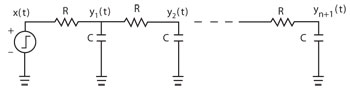
Figure 1 Lowpass section of the (RC)n+1 filter.
The Pulse Generation Method
The shape of a UWB pulse should be designed to achieve low side lobes and compliance to FCC regulation on transmitted power. Pulse shaping is important for the UWB transmission, as it minimizes both adjacent channel interference and inter-symbol interference. Pulse shaping determines the primary characteristic of the distribution of energy within the frequency domain. It concentrates most energy in the main lobe of the pulse spectrum and reduces the side lobe energy, hence reducing the adjacent band interference.5
The most common wideband pulse shape is the Gaussian pulse. Thus, the first attention is directed to the approximated shape of the Gaussian pulse in the CMOS process. The desired step response of the pulse-shaping filter is a Gaussian-shaped pulse and the corresponding frequency response. A well-known technique for approximating a delayed Gaussian waveform is to use a CR-(RC)n filter.6 The Gaussian pulse can be approximated by a realizable CR-(RC)n quasi-Gaussian filter of the form,7
The (RC)n+1 filter shown in Figure 1 has a transfer function given by:
where n+1 is the number of the RC sections and ω= 2πƒ.
Its step response is given by
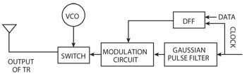
Figure 2 Block diagram of the proposed UWB transmitter.
where K = e−(1/RC)/(RC)n+1 is constant. Equation 3 is similar to Equation 1, so the Gaussian pulse can be approximated by a realizable (RC)n+1 filter.
Transmitter Architecture
The proposed UWB transmitter block diagram is shown in Figure 2. The Gaussian shaping filter produces a pulse train. In this pulse train, the pulse width is inversely proportional to the bandwidth of the required signal. The clock and data inputs are synchronized by the D-flip-flop (DFF). The output of the DFF Q is the synchronized data input. The output P of the Gaussian shaping filter is modulated by the synchronized data to produce the impulse trains S. The switches perform a multiplication between the impulse train S and the carrier signal generated by the voltage control oscillator (VCO). The output can be directly fed to a 50 Ω antenna.
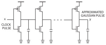
Figure 3 The Gaussian shaping filter.
Gaussian Shaping Filter
The proposed Gaussian shaping filter, shown in Figure 3, is used to approximate a Gaussian pulse and smooth the sharp edge of the clock pulse as explained previously. A CMOS transistor can be modeled as a switch with infinite off-resistance and finite on-resistance. The on-resistance and the capacitance of the transistor determine the transient behavior of an inverter. The additional capacitors of the transistor drains reduce the slope of the rising edge and falling edge of the clock (rectangular) pulse further. The clock pulse is the rectangular pulse
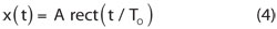
where A is the amplitude and To/2 is the width of the rectangular pulse. Its step response is given by:
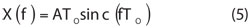
where A is the amplitude of the clock pulse and To is the width of the clock pulse. The step response of the output is
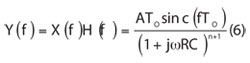
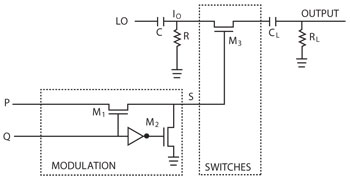
Figure 4 Modulation scheme for PAM.
Equation 6 shows that in the frequency domain, the output of the Gaussian shaping filter has very small side lobes as the number n increases.
Modulation Scheme Selection and Modulator
Figure 4 shows the arrangement for the selectable modulation schemes including PAM. P is the output of the Gaussian shaping filter. C and R are used to filter the DC values of the LO signal from the VCO. The switches facilitate the modulation of the carrier by the Gaussian pulse trains S.
As shown in the figure, P is transferred to S when Q is high, but it is isolated and S is grounded when Q is low. So P is modulated by Q to form S. M2 is used to reduce the noise when M1 is turned off. And lO shifts the pulses of S into the desired frequency. CL and the antenna load (50 Ω) form a high pass filter. For this modulation scheme, the pulses are only produced at the output only when Q = 1.
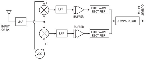
Figure 5 Proposed receiver structure.
The Proposed UWB Receiver
In this article, the receiver is designed for the lower band UWB system, with multi-channel applications. Figure 5 shows the proposed direct conversion receiver (DCR). The architecture of DCR is simple and few external components are needed. It is thus suitable for various multi-band, wideband, and multi-standard applications. A wideband LNA operating from 3 to 5 GHz was designed to amplify the received radio frequency signal. This variable gain LNA has a 50 Ω input impedance for antenna matching and filtering of out-of-band interferers. The passive mixers down-convert the RF signal from the LNA to the baseband I and Q signals by the quadrature LO signals. The passive mixers are selected for their zero power consumption. The RC low pass filter (LPF) removes the high frequency components of the down-converted signals. The full wave rectifiers align the polarities of the pulses in the I and Q paths before the summation. And the comparator, with the inverters, is used after the rectifiers to convert the analog pulse to a digital pulse.
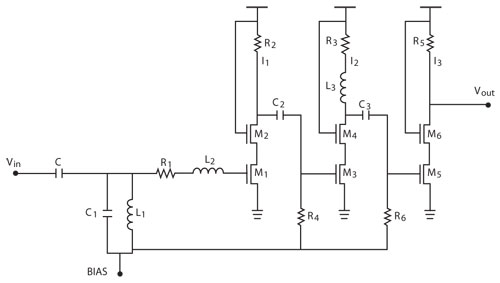
Figure 6 Proposed low power variable gain LNA.
Low Power Variable Gain LNA
The proposed low power variable gain LNA is shown in Figure 6. The first requirement of the LNA is to provide a 50 Ω input impedance for matching the antenna or band select filter to the amplifier. The input matching network of the LNA assists in filtering out the interferers and optimizing the noise performance. The LNA should amplify the radio signal to a desired amplitude that is not too high to affect the linearity or too low to affect the receiver noise figure. A variable gain LNA can be used to optimize the receiver performance.
For the proposed common source LNA, the gain can be adjusted while maintaining low noise figure (NF) and power consumption. The variable gain LNA has three stages. The conventional source inductive degeneration input architecture is not selected, due to its low gain and extra chip area of the source inductor.8 The input impedance of the proposed LNA can be described 8 by:
Figure 7 The passive mixer.
where Ri is the channel charging resistance,9 Rg is the sum of the intrinsic and extrinsic gate resistance and Cgs is the gate-source capacitor of M1. The additional parallel resonator L1 and C1 to the series resonator form a wideband bandpass filter, which gives flat response to the LNA.10 The gain of LNA can be tuned by the bias voltage. The current of M1, M3 and M5 and the overall gain of the LNA are controlled by the bias voltage. The first and third stages have a high gain at low frequencies, and the second stage has a high gain at high frequencies. The size of M1 is designed for proper input matching. The value R2 is critical as it determines the gain of the first stage. The second stage is a cascode common source stage, which provides high frequency gain and better isolation. A series peaking inductor L3 is resonant with the total parasitic capacitance at the drain of M4 and C3.
Mixer and S-QVCO
After the LNA, a passive mixer is used due to its low power and high linearity. A passive mixer dissipates no DC current. In Figure 7, the output Va of the LNA is connected to one of RF terminals of the passive mixer, while the other RF terminal of the mixer is connected to AC ground through the bypass capacitor Cx (5 pF). During the operation of the passive mixer, the transistors act as switches to down-convert the frequency of the signal. In this switching process, the transistors’ on-resistance plays an important role in contributing to the noise figure. In order to turn on and off the transistor, the gate voltage can be described as11

where the source drain terminals are biased at VCM and VTH is the threshold voltage of transistors. The higher aspect ratio of the transistors leads to the better noise performance. In contrast, the small aspect ratio and zero drain-source voltage (VCM) of transistors in the passive mixer core can improve the LO-to-RF isolation.12 VCM is very small and negligible, so the gate voltage is closed to the threshold voltage. To keep the NF of the receiver low, the gain of the LNA must be reasonably high. Thus, smaller aspect ratio transistors are used to give high load impedance to the LNA, and the size of the transistors is optimized against the NF of receiver.
Figure 8 Schematic of the S-QVCO.
Figure 9 Full wave rectifier with CMOS diodes.
The output of the LNA is down-converted by the passive mixer and the series quadrature VCO (S-QVCO) shown in Figure 8. The architecture of the S-QVCO has a low power consumption.13 Due to the low power criterion, the S-QVCO is used for quadrature signal generation and connected with the passive mixer. For this receiver, the required frequency is 4 GHz. A PMOS transistor has a lower flicker noise than an NMOS counterpart, and a p-tail np-core structure is often used in LC VCO. As shown, the circuit has been improved. Here L is 3.5 nH.
The Pulse Detector
After the LPF and the buffer, the outputs of the buffer are not of the same polarity. Detectors that consist of a squarer and an integrator have been published.14,15 The squarer and the integrator are used to produce the same polarity pulses in the UWB receiver. In this article, CMOS full wave rectifiers used as the pulse detector are chosen for such purposes and are shown in Figure 9. The signal goes through M1 and M2 for the positive half cycle and passes the other two transistors for the negative cycle. The low power full wave rectifiers are used to synchronize the polarities of the pulses in the pulse trains. The full wave rectifiers are used to synchronize the polarities of the pulses in the pulse trains and make the same polarity of the pulses when data is “1.” This is new for a UWB receiver. This can be implemented for both the pulse amplitude demodulation and pulse position demodulation.
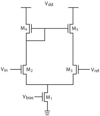
Figure 10 One bit comparator.
Comparator
The comparator is a circuit that compares an analog signal with another analog signal or reference and outputs a binary signal based on the comparison. The quantum voltage comparator consists of two cascade differential pairs with current mirror load.16 Here, the second differential pair of the comparator is replaced by the CMOS inverters. The inverter works as a gain booster to improve the gain of the comparator. Figure 10 shows a one bit comparator that consists of one comparator pair with current mirror load. This comparator with the inverters is used after the rectifiers to convert the analog pulse to digital pulse. The transistor M1 is the switching current source. The differential pair (M2 and M3) of the comparator boosts the input difference voltage in order to provide the voltage difference needed.
Measurement results
The measurement setup for the transceiver is shown in Figure 11. The data input and clock input were sent to the transmitter and the Gaussian pulse train was measured at the output of the transmitter. The output of the transmitter was connected to the receiver through an attenuator, which accounts for the power propagation loss in the air in a wireless connection. The received power can be determined by the emitted power from the transmitter and the distance between the transmitter and the receiver if the antenna gain is negligible. The receiver demodulates the attenuated signal and produces detected data at the output of the receiver. The die photograph of the whole transceiver is shown in Figure 12. The chip size is 2.4 x 1.3 mm.

Figure 11 Setup of simulation measurement for the complete transceiver.
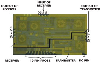
Figure 12 Photograph of the fabricated single chip transceiver.
The approximate single Gaussian pulse shown in Figure 13 is measured at the output of the transmitter. The Vpp of the transmitter is 125 mV and the center frequency is 4 GHz. The figure also shows the input return loss of the receiver. The measured S11 is less than –10 dB from 2 to 6 GHz. For a 1.8 V power supply, the current consumptions of the transmitter and receiver are 3 and 14 mA, respectively.
As the measurements were performed on wafer, the output of the transmitter is passed through an attenuator to account for the propagation loss then looped back to the receiver. In Figure 14, the data input (a) and the clock input (b) of the transmitter are shown, as well as the time-domain response of the proposed transmitter (c) with a pulse repetition frequency of 52 MHz input at a 1.8 V supply voltage, while (d) is the demodulated output of the receiver. The whole receiver achieves a 39 dBm gain. The tuning range of the center frequency of S-QVCO in the receiver is 1 GHz. The noise figure of the whole transceiver is 8 dB.
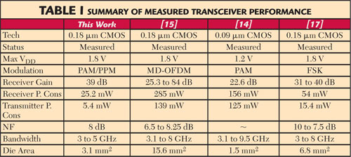
The proposed transceiver is compared with other receivers in Table 1. As shown, the proposed transceiver has the lowest power consumption. Although the area of Zhang’s transceiver14 is half of the proposed transceiver, its power consumption is five times the power consumption of the proposed transceiver and its transmitter power consumption is twenty-three times that of the proposed transmitter. Additionally, the gain of the proposed receiver is higher by 16.4 dB. The several nanosecond narrow pulse train was demodulated in the proposed receiver. The small narrow analog pulse has been demodulated into the rectangular digital in the proposed receiver. This is an additional contribution of this proposed transceiver. The demodulation of the short pulse is usually not dealt with in other publications. This receiver can be used for both pulse amplitude modulation and pulse position modulation.
Conclusion
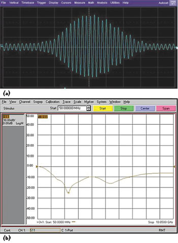
Figure 13 Single pulse at the output of the transmitter (a), S11 of the LNA at the input of the receiver (b).
In this article, a new design of a single chip transceiver is presented. The proposed transceiver can operate at various frequencies, determined by the S-QVCO. The design frequency is from 3 to 5 GHz of the lower band of the UWB system. This transceiver can be used for the multi-band UWB system, consumes a low power and occupies a small size for both transmitter and receiver. A new proposed Gaussian pulse filter is used in the transmitters. It consumes low power and can obtain the approximate Gaussian pulses. A simple and low power modulation scheme was also designed for transmitter.
The main advantage of the proposed receiver is that both the size and the power consumption are small, while maintaining sufficient gain. The rectifiers are used to polarize the pulse polarity in the UWB receiver for the first time. The pulses can be demodulated by using the CMOS full wave rectifiers that consume a low power and occupy a small area in the chip. This is the first innovation point in the receiver. The variable gain LNA has been investigated also. The gain of these three stages LNA could be tuned by the bias voltage in the LNA. The LNA offers sufficient gain to keep a low noise figure for the whole receiver.
References
- “Revision of Part 15 of the Commission’s Rules Regarding Ultra-wide-band Transmission Systems,” FCC, Washington, DC, 2002, FCC report and order, adopted February 14, 2002, released July 15, 2002.
- A.A. Abidi, “The Path to the Software-Defined Radio Receiver,” IEEE Journal of Solid-State Circuits, Vol. 42, No. 5, May 2007, pp. 954-966.
- G. Cusmai et al., “A 0.18-µm CMOS Selective Receiver Front-end for UWB Application,” IEEE Journal of Solid-State Circuits, Vol. 41, No. 8. August 2006, pp. 1764-1771.
- F.S. Lee and A.P. Chandradasan, “A BiCMOS Ultra-Wideband 3.1 to 10.6 GHz Front-end,” IEEE Journal of Solid-State Circuits, Vol. 41, No. 8, August 2006, pp. 1784-1791.
- M. Ghavami, L.B. Michael and R. Kohno, “Ultra Wideband Signals and Systems in Communication Engineering,” John Wiley & Sons Ltd, Chichester, UK, 2007.
- Z.Y. Chang and W.M.C. Sansen, “Low-Noise Wide-Band Amplifiers in Bipolar and CMOS Technologies,” Ch. 5, Kluwer, Norwell, MA, 1991.
- E. Fairstein, “Linear Unipolar Pulse-Shaping Networks: Current Technology,” IEEE Transaction on Nuclear Science, Vol. 37, No. 2, Pt. 1, April 1990, pp. 382-397.
- M. Shouxian, M. Jian-Guo, Y.K. Seng and D. Manh Anh, “A Modified Architecture Used for Input Matching in CMOS Low Noise Amplifiers,” IEEE Transactions on Circuits and Systems, Vol. 52, No. 11, November 2005, pp. 784-788.
- T. Manku, “Microwave CMOS-device Physics and Design,” IEEE Journal of Solid-State Circuits, Vol. 34, No. 3, March 1999, pp. 277-285.
- A. Ismail and A.A. Abidi, “A 3-10 GHz Low Noise Amplifier with Wideband LC-Ladder Matching Network,” IEEE Journal of Solid-State Circuits, Vol. 39, No. 12, December 2004, pp. 2269-2277.
- T.K. Nguyen et al., “ A Low-Power RF Direct-Conversion Receiver/Transmitter for 2.1-GHz-Band IEEE 802.15.4 Standard in 0.18-µm CMOS Technology,” IEEE Transactions on Microwave Theory and Techniques, Vol. 54, No. 12, December 2006, pp. 4062-4071.
- C.G. Tan, “A High-performance Low-power CMOS Double-balanced IQ Down-conversion Mixer for 2.45 GHz ISM Band Application,” 2003 IEEE Radio Frequency Integrated Circuits Symposium Digest, pp. 457-460.
- V. Krishna et al., “A Low Power Fully Programmable 1 MHz Resolution 2.4 GHz CMOS PLL Frequency Synthesizer,”2007 IEEE Biomedical Circuits and Systems Conference Digest, pp. 187-190.
- F. Zhang, A. Jha, R. Gharpurey and P. Kinget, “An Agile, Ultra-wideband Pulse Radio Transceiver with Discrete-time Wideband-IF,” IEEE Journal of Solid-State Circuits, Vol. 44, No. 5, May 2009, pp. 1336-1351.
- H. Zheng, S. Luo, D. Lu, C. Shen, T. Chan and H.C. Luong, “A 3.1 GHz-8.0 GHz Single-Chip Transceiver for MB-OFDM UWB in 0.18-µm CMOS Process,” IEEE Journal of Solid-State Circuits, Vol. 44, No. 23, February 2009, pp. 414-425.
- J. Yoo, K. Cho and J. Ghaznavi, “Quantum Voltage Comparator for 0.7 µm CMOS Flash A/D Converters,” 2003 IEEE Annual Symposium on VLSI Digest, pp. 280-281.
- M.U. Nair, Y. Zheng, C.W. Ang, Y. Lian, Xiaojun Yuan and Chun Huat Heng,
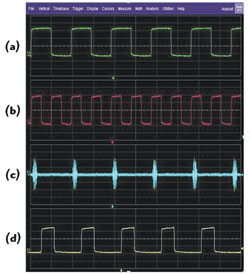
Figure 14 Data input of the transmitter (a), clock input of the transmitter (b), received pulse train at the receiver (c), output of the receiver (d).
“A Low SIR Impulse UWB Transceiver Utilizing Chirp FSK in 0.18 µm CMOS,” IEEE Journal of Solid-State Circuits, Vol. 45, No. 11, November 2010, pp. 2388-2403.
Caixia Chenreceived her B.Eng. (1st Honors) from Nanyang Technological University (NTU), Singapore, in 2006. She is expected to get her Ph.D. degree in 2012 from Nanyang Technological University. Since October 2010, she has been working at Avago Technologies as an R&D engineer. Her research interests include design and implementation of the ultra-wideband transmitter and receiver based on CMOS for wireless communication.
Manh Anh Do received his B.E. (Honors) degree and a Ph.D. degree in electrical engineering from the University of Canterbury, Christchurch, New Zealand, in 1973 and 1977, respectively. Between 1977 and 1989, he held various positions, including as a design engineer, production manager, and research scientist in New Zealand and a senior lecturer with the National University of Singapore, Singapore. He joined the School of Electrical and Electronic Engineering, Nanyang Technological University (NTU), Singapore, as a senior lecturer in 1989 and obtained the Associate Professorship in 1996 and Professorship in 2001. Between 1995 and 2005, he was head of the division of circuits and systems, NTU. He was the director of center for integrated circuits and systems from 2007 to 2010. He is currently a member of the NTU Research Council. His current research interests include mobile communications, RFIC design and mixed-signal circuits.
Kiat Seng Yeo received his B.Eng. (Honors) (Elect) in 1993 and Ph.D. (Elect. Eng.) in 1996, both from Nanyang Technological University, Singapore. In 1996, he joined the School of Electrical and Electronic Engineering, Nanyang Technological University, Singapore, as a lecturer and became an assistant professor in 1999 and an associate professor in 2002. He has been appointed head of circuits and Systems for a period of six years from 1 July 2005.
Chirn Chye Boon received his B.E. (Honors.) (Elect.) in 2000 and his Ph.D. (Elect. Eng.) in 2004 from Nanyang Technological University (NTU), Singapore. In 2005, he joined NTU as a Research Fellow and became an assistant professor in the same year. Before that, he was with Advanced RFIC, where he worked as a senior engineer. He specializes in the areas of radio frequency (RF) and mm-wave circuits and systems design for biomedical and communications applications.
Wei Meng Lim received his B.E. (Honors) and M.E. degrees from Nanyang Technological University (NTU), Singapore, in 2002 and 2004 respectively. Upon his graduation, he joined the School of Electrical and Electronic Engineering, NTU, as a research staff. His research interests include RF circuit designs, RF devices characterization and modeling.