
Zero-IF receivers are not new; they have been around for some time and are prominently used in cell phone handsets. However their use in high performance receivers, such as those in wireless base stations, has had limited success. This is due primarily to their limited dynamic range and that they are less understood. A new wide bandwidth zero-IF I/Q demodulator helps to relieve the dynamic range and bandwidth shortcomings for main as well as digital pre-distortion (DPD) receivers and enables 4G base stations to cost effectively address the ever-increasing bandwidth needs of mobile access. This feature covers how to optimize performance by minimizing the IM2 nonlinearity and DC offset that reduce the dynamic range of zero-IF receivers, thus offering a viable alternative to an otherwise challenging design.
Pushing Ever Wider Bandwidth
Until recently, most base stations needed to only deal with a 20 MHz wide channel bandwidth, typically allocated to various wireless carriers. Associated with this 20 MHz channel is a companion 100 MHz bandwidth DPD receiver to measure intermodulation distortion spurs up to fifth-order for effective distortion cancellations. These requirements can generally be met effectively with high-IF (heterodyne) receivers. Nowadays though, such designs become much more challenging with industry trends pushing for base stations that support operation over the entire 60 MHz bands. Accomplishing this feat has significant cost saving implications for the entire wireless manufacturing, installation and deployment business model.
To accommodate the three times increase in bandwidth, the DPD receiver bandwidth has to increase from 100 to 300 MHz. In 75 MHz bands, the DPD bandwidth grows to a staggering 375 MHz. The design of receivers that can support this bandwidth is not trivial. Noise increases due to the wider bandwidth, gain flatness becomes more difficult to achieve, and the required sampling rate of A/D converters increases dramatically. Furthermore, the cost of such higher bandwidth components is appreciably higher.
The modest bandwidth of a traditional high-IF receiver is no longer sufficient to support the 300 MHz or higher DPD signal with typically ±0.5 dB gain flatness. The 300 MHz baseband bandwidth would require choosing an IF frequency of 150 MHz at a minimum. It is not trivial to find an A/D converter capable of a sampling rate upward of 600 Msps that is reasonably priced, even at 12-bit resolution. One may have to compromise and resort to a 10-bit converter.
New I/Q Demodulator Eases Bandwidth Constraints
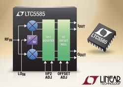
Linear Technology’s LTC5585 I/Q demodulator is designed to support direct conversion, thus allowing a receiver to demodulate the aforementioned 300 MHz wide RF signal directly to baseband (see the following link for I/Q demodulator theory of operation – www.mwjournal.com/IQtheory). The I and Q outputs are demodulated to a 150 MHz wide signal, only half the bandwidth of a high-IF receiver. In order to attain a passband gain flatness of ±0.5 dB, the device’s -3 dB corner must extend well above 500 MHz.
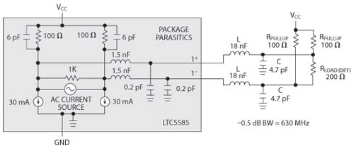
Figure 1 Baseband output equivalent circuit for bandwidth extension with L = 18 nH and C = 4.7 pF.
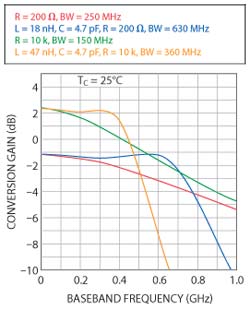
Fig. 2 Conversion gain vs. baseband frequency with differential loading resistance and L-C bandwidth extension.
The LTC5585 supports this wide bandwidth with a tunable baseband output stage. The differential I and Q output ports have a 100 Wpull-up to VCC in parallel with a filter capacitance of about 6 pF (see Figure 1). This simple R-C network allows for the formation of off-chip lowpass or bandpass filter networks to remove high-level out-of-band blockers and equalization of gain roll-off the baseband amplifier chain that follows the demodulator. With a 100 Wdifferential output loading resistance in addition to the external 100 Wpull-up resistors, the -3 dB bandwidth reaches 840 MHz.
Baseband Bandwidth Extension
A single L-C filter section can be used to extend the bandwidth of the baseband output. Figure 1 shows the chip’s baseband equivalent circuit with baseband bandwidth extension. With 200 W loading, the 0.5 dB bandwidth can be extended from 250 to 630 MHz using a series inductance of 18 nH and a shunt capacitance of 4.7 pF. Figure 2 shows the variety of output responses that are possible with different loading. One response is with differential loading resistances of 200 Wand 10 kW. For 10 kWloading, the -0.5 dB bandwidth can be extended from 150 to 360 MHz using a series inductance of 47 nH and a shunt capacitance of 4.7 pF.
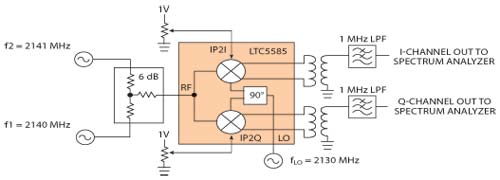
Figure 3 Test set-up for IIP2 calibration with 1 MHz lowpass filters to select the IM2 component.
Second-Order Intermodulation Distortion Spurs Matter
In a direct conversion receiver, the second order intermodulation distortion products (IM2) fall directly in-band at the baseband frequencies. Take, for example, two equal power RF signals, f1 and f2, spaced 1 MHz apart at 2140 and 2141 MHz, respectively, while the LO is spaced 10 MHz apart at 2130 MHz. The resultant IM2 spur would fall at f2 - f1, or 1 MHz. The LTC5585 has the unique ability to adjust for minimum IM2 spurs independently on the I and Q channels by using external control voltages. Figure 3 shows a typical set-up for IIP2 measurement and calibration. The differential baseband outputs are combined using a balun and the 1 MHz IM2 difference frequency component is selected with a lowpass filter to prevent the strong main tones at 10 and 11 MHz from compressing the spectrum analyzer front end. Without the lowpass filter, 20 to 30 dB of attenuation and long averaged measurement times are necessary on the spectrum analyzer to attain a good measurement. As shown in the output spectrum of Figure 4, the IM2 component predictably falls in-band at 1 MHz. The plot also shows the IM2 product before and after adjustment, reducing the spur level by approximately 20 dB by adjusting the control voltages on the IP2I and IP2Q pins. This adjustment reduces the IM2 spur down to a level of -81.37 dBc.
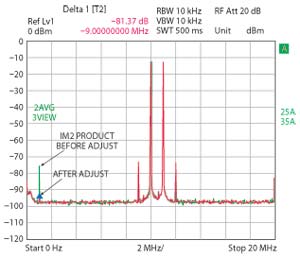
Fig. 4 Output spectrum without lowpass.
With this IIP2 optimization capability, two possible strategies of IP2 calibration may be considered. One can be a set-and-forget calibration step performed at the factory. In this case, a simple trim potentiometer for each adjustment pin suffices, as illustrated in Figure 3. Alternatively, an automatic, closed loop calibration algorithm can be implemented in the software which allows the equipment to be calibrated on a periodic basis. For DPD receivers that are already monitoring their transmitters’ output, this is trivial as the transmitters can easily generate the two test tones. For main receivers, this calibration may involve additional hardware to loop back the two test tones to the receiver channel. In any event, these can all be performed during an off-line calibration cycle. Such an approach would take into account the actual operating environmental factors that may affect the base station’s performance.
Optimizing A/D Converter Dynamic Range
A similar adjustment capability is also integrated into the chip to zero out the I and Q’s DC output voltage. DC offset, a product arising from internal mismatch and self-mixing of the LO and RF input leakages, can diminish the ADC’s dynamic range when the signal chain is DC coupled throughout. To illustrate, a modest 10 mV of output DC offset voltage, when passed through a 20 dB gain stage, would result in 100 mV of DC offset at the input of the A/D converter. With 2 Vp-p input range of a 12-bit ADC, this amount of DC offset represents 205 LSBs of headroom reduction, or effectively reducing the ADC’s dynamic range by 0.9 dB.
To minimize the leakage between the LO and RF inputs, care should be taken to isolate these two signals. In the PCB layout, separate these two signal traces from one another to prevent cross-coupling. The LO signal, even if there is measurable leakage to the RF port, will self-mix to form a DC offset term at the output. Fortunately the LO level is usually constant, so the DC offset voltage is also constant and can be easily canceled by the adjustment. More problematic is the RF input, which can vary over wide signal levels. Any signal leakage to the LO input would self-mix and produce a dynamic DC offset voltage as the signal varies. This will distort the demodulated signal. So keeping the leakage small will help to reduce the DC offset to a minimum.
Potential Cost Benefits of Direct Conversion Receivers
A zero-IF receiver is particularly compelling due to its potential cost savings. As mentioned above, the RF signal demodulates to a low frequency baseband. At lower frequencies, the design of the filter becomes easier. Furthermore, zero-IF demodulation produces no image at the baseband, thus eliminating the need for a relatively expensive SAW filter. Perhaps most attractive of all is that the ADC sampling rate can be significantly reduced. In our example above, the 150 MHz I and Q baseband bandwidth can be effectively addressed with a dual 310 Msps ADC such as Linear Technology’s LTC2258-14, without resorting to a much more expensive higher sampling rate ADC.
As the bandwidth and performance of wireless receivers increase, a new wideband quadrature demodulator offers an alternative approach that helps to address its architectural shortcomings and raises the level of receiver performance while driving a compelling cost metric.
Linear Technology Corp.,
Milpitas, CA
(408) 432-1900,
www.linear.com.