
As discussed in part one of this article, the measurement of very good VCOs at large frequency offsets is limited by the spectrum analyzer’s dynamic range. This limitation can be overcome by using carrier filtering and selective amplification of noise at the offset frequency of interest. The bandpass filter (BPF) must have a very sharp roll-off to provide enough rejection to the carrier signal compared to the desired offset frequency, as shown in Figure 1. Modern monolithic VCOs use switched reactance resonators to achieve wide tuning range along with low noise performance. Therefore, it is important to verify the design at different carrier frequencies as Leeson’s rule may not be directly applicable, and a particular switch combination may be too lossy to give good phase noise. The filter would need to be tunable to measure phase noise of different carrier frequencies.

Fig. 1 Carrier filtering and selective amplification of noise.
The filter roll-off may change each time it is tuned and if the impedance presented to it changes. Therefore, stop-band rejection needs to be re-measured every time it is re-tuned. The filter’s selectivity is accompanied by a poor S11 in the stop-band. This is how filters provide a frequency selective impedance match and hence a frequency selective power transfer to the load. The carrier signal that falls in the filter stop-band gets reflected back to the VCO and can cause severe load pulling, thus destabilizing the device under test (DUT).
To alleviate this problem, an attenuator can be used between the VCO and the filter. This reduces the signal power in both directions and minimizes the reflections going back into the VCO. At the same time, too much attenuation decreases the DUT signal and noise levels towards the fundamental noise limit, which may increase the measurement error.
An isolator will do the job without too much attenuation, but it is a narrowband device and may need to be replaced if the DUT needs to be characterized over a very wide frequency band, such as a triple- or quad-band VCO. A low noise, low gain amplifier with a reasonable S12 and high P1dB is another choice that can provide a broadband 50 Ω impedance and adequate isolation.
Figure 2 shows how a carrier is placed outside the filter passband and the lower noise sideband is selectively amplified. The measurement is done in two steps. First, the phase noise is measured with an attenuated carrier just like in the direct spectrum analysis approach. The instrument is set in the low noise measurement mode that is minimum attenuation and possibly some amplification. Then the carrier is moved to the noise offset frequency to measure the filter rejection to carrier with respect to the noise offset frequency, while the instrument is set in high IP3 mode, that is with minimum amplification and/or high attenuation.
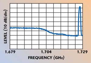
Fig. 2 Measurement example using a carrier filtering method.
Figure 3 shows a cascade of an amplifier, two filters and a 3 dB pad used between the DUT and the spectrum analyzer. A careful measurement setup can give good results and this method can be used to measure the combined effect of AM and PM noise. It can help to verify the measurements done using other methods discussed in the following sections. It can also help to conclude the absence of AM noise if this measurement agrees with a pure phase noise measurement.
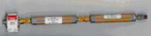
Fig. 3 Cascade of an amplifier, two filters and a 3 dB pad between the DUT and a spectrum analyzer.
This is a very basic improvement over the direct spectrum analysis. All measurements are done at high frequencies. The more sophisticated techniques, discussed below, use phase or frequency demodulation of the noise. Direct demodulation to baseband is possible for frequencies up to 2 to 3 GHz. For higher frequencies, a down-conversion may precede demodulation.
PHASE DETECTION
Phase detection is the most common demodulation method used in different types of phase noise measurements. Consider the equation representing PM/FM of an ideal sinusoid.

A basic approach is to detect the phase variations in Δφ(t) by multiplying the above signal with a pure sinusoid, assuming it exists
![]()
for a small magnitude of Δφ(t).
An easy way to understand this method is to consider the case of a high measurement offset from the carrier, as shown in Figure 4. A narrow bandpass filter gives enough attenuation to noise at high offset frequencies. Therefore, at the mixer output, the measured noise at those offsets and above is due to the phase noise of the original signal. Phase quadrature also must be maintained between the input ports of the mixer, which is accomplished by a phase shifter.

Fig. 4 Cavity resonator as noise filter and delay line.
The complexity of this method increases for measurements at low frequency offsets from the carrier because the filter bandwidth needs to be much smaller. Some setups use cavity resonators for such measurements. When using high Q cavities or bandpass filters for measurement offsets well within the passband, the group delay of the filter makes this method similar to the delay line discriminator.
Mixer as Phase Detector
Most of the measurement techniques discussed in the following sections use a double-balanced mixer as a phase detector; therefore, it is important to understand this component. A simple way to understand the operation of the mixer as a phase detector is to feed its LO and RF ports with the same signal with a variable phase shifter at one of these ports. The IF port gives out a DC signal (if the IF bandwidth extends down to DC and the output is DC coupled). As the phase shift is varied, the DC level at the IF port varies. Over a 0° to 360° phase shift, the DC output completes one sine cycle, as shown in Figure 5.

Fig. 5 Phase detector output voltage vs. the input’s phase difference.
Only the lower sideband is considered here and the sum frequencies are filtered out. This is precisely what happens in a downconverter when the frequency of the RF signal is slightly different from the LO frequency. The phase difference between these two signals varies with time and generates an IF with a frequency that is the difference between the RF and LO frequencies (note that the sum frequency term is filtered out). If the RF or LO signals have random phase fluctuations (modulation), they will also show up as phase, and hence frequency fluctuations of the IF signal. A passive double-balanced mixer typically consists of four diodes and two transformers, which also provide the desired match. Even if the LO source is a sine wave generator, the LO port is driven so hard in compression that the LO waveform, in effect, looks like a square wave that alternately switches two of the four diodes at a time. These mixers need higher LO drive levels compared to active mixers, but provide very good levels of isolation. The peak output amplitude depends on the input RF level and the conversion loss. The conversion loss, in turn, varies with LO level if the LO drive is insufficient to fully turn on the switching diodes. Ohmic loss in the diodes and transformers adds to conversion loss from RF to IF. In single-sideband (SSB) applications, half of the power in the unwanted sideband gets filtered out. Except for conversion loss, a passive double-balanced mixer can be considered as an ideal multiplier for mathematical calculations. When the LO and RF ports are fed with adequate amplitude, the output depends only on the phase difference and not on input amplitude variations. Thus, the AM noise is suppressed and the measurement accounts for only phase fluctuations of the DUT signal.
The wideband noise at RF frequencies introduced by this mixer is negligible. The noise figure is defined as the signal-to-noise ratio (SNR) degradation due to the insertion loss that pushes the noise density of interest towards –174 dBm/Hz. At low frequencies, however, these switching diodes add a substantial amount of flicker noise, which can limit the low frequency measurements if the phase detector performance is worse compared to the phase noise of the DUT. This situation is very similar to the case of zero-IF receivers in which mixer flicker noise is a matter of concern.
Delay Line Discriminator

Fig. 6 Delay line discriminator.
A system level diagram of a delay line discriminator is shown in Figure 6. An FM signal

is split into two channels. A 3 dB split is commonly used but is not absolutely necessary. The mixer inputs are

and

where

The mixer output as seen in time domain is given by
![]()
from which the high frequency terms are filtered out. Since the delay line and the phase shifter together keep the mixer inputs in quadrature, the phase relation can be written as

where k is an integer.
Now the mixer output can be rewritten as
This signal needs to be amplified before spectrum analysis. The equation can be further simplified and expressed as

Notice that the first term is a constant and the second term is a phase-shifted sinusoid with the phase shift a function of τ. This time domain signal can be expressed in the frequency domain as

The amplitude of the demodulated signal is a function of offset frequency fm and delay τ. The frequency response of the measurement setup can be plotted using

The magnitude of the output signal is of the form

and is shown in Figure 7 for different values of delay, τ. This includes the DUT modulation index.
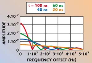
Fig. 7 Frequency response of the measurement setup.
For FM modulation, the modulation index (and hence the sideband level) decreases with increasing fm, as seen in Equations 3 and 6. Therefore, the discriminator output plotted also seems to decrease with increasing fm. If the modulation index at the input of the discriminator is kept constant for all fm, the output will vary as |sin(πfmτ)| and is plotted in Figure 8.

Fig. 8 Discriminator output with a constant modulation index of the input source.
For πfmτ < 0.5, sin(πfmτ) ~ πfmτ and sinc (fmτ) ~ 1, a single calibration can be used for measurements at multiple offsets for fm < 1/2πτ.
The measurement error increases for higher frequency offsets. This error has two contributions — one is due to the dependence of the modulation index on frequency and the other is the response of the discriminator itself. The net error corresponds to sinc(fmτ). It is possible to compensate for this response, so that a single calibration would suffice for measurements at multiple offsets. For the best results that account for non-flat frequency responses of the different system blocks, however, it is better to calibrate for each individual offset frequency.
Practical Limitations of a Narrowband Measurement Circuit
To gain more insight into the demodulation process, Equations 4 and 5 are expanded using Equation 6. The scaling factor Ac/2 is ignored.

where

The scaling factors m, u and l have been introduced to take into account the frequency-dependent amplitude response.
The terms associated with second channel output from the splitter undergo a phase shift due to the combined effect of the phase shifter and delay line. Assuming that the phase shifter’s phase response is constant over frequency (a practical case is explained later), the delay line is the only element that gives a frequency-dependent phase shift. For a delay time τ, the phase angle for upper and lower sidebands and carrier can be written as (ω + ωm)τ, (ωc – ωm)τ and ωcτ, respectively.
The mixer acts as a phase detector and the delay line can be seen as a frequency-to-phase converter. This intuitively explains why the demodulation gain increases with τ. It is important to note that for a longer delay line, the attenuation is also higher and that reduces the signal level input to the phase detector.
Using
![]()
and

and

to calculate the expression for mixer output. After simplifying and rejecting the high frequency terms,
From Equation 13, if the bandwidth of the signal processing circuits is not wide enough, the resulting amplitude difference between upper and lower sidebands at the mixer input can produce a DC shift at the mixer output. This can happen when measurements are done at large frequency offsets. Therefore, it is important to use wideband circuits to ensure m = u = l, so that Equation 13 reduces to the form of Equation 9. The original modulated signal is recovered at the mixer output as a sum of the two tones at the same frequency but out of phase. This phase difference is proportional to ωmτ. This simplified analysis assumes that the phase shifter phase response does not vary with frequency, which is not true for practical phase shifters. The non-zero phase slope of a real phase shifter may reduce or enhance the effect of θ, depending on whether the phase shifter is connected in series with the delay line or in the other signal path.
m, u and l may have different values, but if they remain constant between the calibration and measurement, the measurement error can be negligible, as long as the modulation sidebands at the input of the discriminator are equal in amplitude and can be measured accurately.
DC offset: The two signals at the mixer input should be in phase quadrature, failing which, there will be a DC voltage present at the IF output. If the DC shift is small, the measurement can still be made accurately as long as the RF-LO phase relationship remains the same during measurement and calibration.
In the case of free-running VCO measurements, the carrier signal may slowly drift away from the frequency at which measurement was started. A change in frequency also changes the phase shift seen by the signal of interest. Usually, a free-running VCO is measured with a very tight low pass filter (LPF) at the tuning port and will drift monotonically in one direction. To analyze this drift, the previous analysis is repeated by using an extra factor φ, which denotes the phase shift due to frequency drift. For the sake of simplicity, the effect of the delay line only is analyzed.
The equations with m = u = l and phase shift for the different frequency components can be rewritten. For the upper sideband the phase shift is
![]()
for the center frequency, the phase shift is
![]()
and for the lower sideband, the phase shift is
![]()
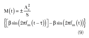
Again, M(t) = X1(t)X2(t).
The mixer is again considered an ideal multiplier. The high frequency terms are filtered. The total DC at the output of the mixer is given as

For low phase noise levels, particularly at very high offsets, the DC voltage at the mixer output varies as
![]()
Simplifying the rest of the terms, the demodulated signal at frequency fm that was originally used to frequency modulate the DUT is given by

Thus, the output signal level at a given offset fm varies as the cosine of the phase shift.
Theoretically, for this type of measurement error to be less than a dB, f must be less than 27°. The approximate allowable frequency drift for this condition is

System Calibration and Measurement Errors
One obvious choice is to measure the frequency response of each measurement component and then to calculate the system response. The phase detector gain may be found experimentally near its zero crossing point as the slope of the curve of the phase detector output. The noise level of the DUT can then be calculated from the measured noise and the discriminator transfer function. This can be a tedious task.
Calibration can also be performed by frequency modulating the DUT with a sinusoid of frequency fm. The modulation of the DUT is then disabled and the output due to the DUT noise is measured.
An alternative to DUT modulation is to use an FM signal generator at the system input for calibration. Note that even if the LO signal drives the mixer into hard saturation, the RF level into the mixer will be several dBs below the LO level, primarily due to the delay line or phase shifter loss. The problem with this alternative approach is the possibility of an impedance change at the input of the measurement system, which can vary the amount of power transferred to the phase detector between the calibration and actual measurement, altering the phase detection gain. This may affect the DC and AC levels out of the mixer. A major advantage of using VCO modulation for calibration, instead of using an external signal generator, is that the main RF signal path is never disconnected and the measurement and calibration conditions are exactly the same.
For measurements at large frequency offsets, such as 20 MHz, simple things like frequency modulation of the carrier can be tricky, since most signal generators do not have internal FM modulators that go as high as 20 MHz. If the user has a choice, the best method is to feed the control line of the VCO using a signal generator. However, the loop filter must be protected from getting loaded by the internal impedance of the modulating source.
Even though discriminators are best suited for measuring noisy sources in an open loop mode, the user may want to measure a locked VCO. In certain cases, when very low noise levels are to be measured at large offset frequencies, a harmonic of the reference spur may fall very close to the measurement point if the PLL comparison frequency is smaller than the measurement offset and the loop bandwidth is not small enough. Such low level spurs are not noticeable during normal spectral analysis of PLLs since they are far below the analyzer’s noise level. These spurs can also be displaced from the point of measurement by slightly offsetting the phase detector frequency by changing the reference count value or by changing the reference frequency itself.
This also means that this technique is useful not only for phase noise measurements, but also for detecting such spurious signals, which may otherwise go undetected during direct spectrum analysis.
LMX2604 Measurements
The LMX2604 chip has two VCOs, and has been designed to suit a GSM transmit architecture that uses closed loop modulation within an offset PLL in the GSM, DCS and PCS bands.4
The phase noise plot in Figure 9 shows the performance of two VCOs at the upper edge of the GSM and PCS bands. Frequency offsets below 1 MHz were measured using an Agilent 4352S and, for offsets beyond that, a delay line discriminator was used. This VCO has an output power level of +6 dBm. There are two main ports for the GSM and DCS/PCS output, and there is a separate port for feeding the mixer in the offset PLL circuit. This port feeds the PLL N counter in the test circuit.
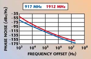
Fig. 9 Phase noise performance of the LMX2604.
Measurement Circuit
The implementation is the same as shown for the delay line discriminator. The harmonic balance simulation was done using ADS to verify the theoretical derivations, the effect of each system block on noise measurements and the DC offset at the output of the phase detector. Different blocks were implemented using distributed transmission line circuits. Figure 10 shows the PCB realization of these circuits. A five-section coupler was used to sample the calibrating signal fed to the RF amplifier. The RF amplifier is a low noise 50 Ω block with a gain of 10 dB, a noise figure of 2.2 dB and a P1dB of +20 dBm. A Lange coupler was used as a power splitter after the initial amplification. A level 7, double-balanced passive mixer was used as a phase detector, followed by an IF filter. The IF filter bandwidth needs to be wider than the maximum offset frequency of interest, while rejecting the carrier harmonics. A combination of lumped elements and transmission line resonators were cascaded to get a stop-band ranging from 500 MHz to 6 GHz in order to keep the IF amplifiers from getting saturated, particularly when wideband devices are used. If a wider bandwidth of operation is desired, multiple sections are needed and the circuit size increases. A ceramic substrate with εr = 10 was selected to keep the circuit size small, while allowing suitable dimensions for the Lange coupler (5 mil line width with 5 mil spacing). The first prototype used hand-soldered wires for the Lange coupler, instead of wire-bonds, and the circuit performed very well. The delay line is external to this PCB and the setup can easily cover frequencies ranging from approximately 1 to 3 GHz, with a minor change in lumped capacitors in the phase shifter circuit. A voltage-controlled phase shifter was implemented using the same Lange coupler as a 3 dB 90° hybrid in conjunction with two identical varactor-tuned reflection networks.6

Fig. 10 Measurement circuits fabricated on PCB.
Figure 11 shows the impedance plots of the reflection networks used in the tunable phase shifter. The insertion loss of this phase shifter depends on the insertion loss of the coupler circuit and the parasitic series resistance of the varactor diodes. It is possible to get very large values of phase shift from a single 3 dB hybrid by resonating the reflection networks, but there is a trade off between the phase shift and insertion loss. Multiple sections can help to achieve multiple resonance points, and give a large phase shift range over a very wide frequency band. However, the real part of impedance also varies sharply near the parallel resonance. It is around this point that the insertion loss is maximum because reflections are not perfect and some signal power is dissipated in this circuit.

Fig. 11 Reflection circuit with variable angle of reflection.
For this application, a 180° phase shift would suffice. There are two such circuits cascaded to cover the desired phase shift over a wide range of frequencies. A small length of cable can also be switched-in for coarse phase adjustments and then fine-tuning can be done with an even lower phase shift range. The phase shift range with respect to tuning voltage and the maximum insertion loss over tuning range for different frequencies are shown in Appendix A.

The electrically tunable phase shifter is much easier to work with, compared to a manually tunable phase shifter. One major design constraint is that the rate of change of phase should not vary significantly over a bandwidth as large as the measurement offset.
This setup needs a careful calibration but is not very difficult to operate. Depending on the DUT specifications, minor variations in the setup may be needed. This setup does not result in a nice graph, compared with instruments available, but this is a very simple, compact and cost-effective solution. A careful calibration can give accurate results. The setup was automated to measure (and calibrate) the phase noise at three different frequency offsets for nine different carrier frequencies in the GSM, DCS and PCS bands.
Other Methods for Phase Noise Measurement
A phase-locked loop can be used to automatically correct for quadrature phase using a reference oscillator. At the phase detector output, the down-converted noise is available for amplification and analysis. Since the in-band closed loop transfer function presents the same gain to the phase noise from both oscillators, the performance of the reference oscillator needs to be better than the DUT. As in the case of the delay line method, this method also needs calibration to account for phase detector gain, loss and the noise contribution of different circuit blocks.
The PLL method is considered better than the delay line discriminator for measuring locked devices or VCOs with low noise floor at lower offset frequencies. One reason is that the discriminator transfer function suppresses the noise at a rate of 20 dB/decade below its peak response frequency. Another reason is that the reference source, in the PLL method, can itself be a PLL with a loop bandwidth wider than the frequency offset of interest. Thus, for low frequency offsets, the discriminator technique can be used for measuring noisy oscillators and handles frequency drifts very well. For low frequency offset measurement of low noise oscillators, the peak response point of a delay line discriminator can also be moved to a lower frequency by increasing the delay. The price paid is the increased attenuation. The delay line characteristics depend on length, dielectric constant and physical construction of the transmission line. It is possible to use a microstrip or a stripline with low propagation velocity of transmission line structures on a very high εr substrate, but the problems include a limited band of operation and group delay variation with frequency. For best performance, the delay should be non-dispersive and nothing beats a coaxial cable in that sense.
Conclusion
A systematic approach has been presented for understanding the basics of phase noise and explaining measurement methods of varying complexity. Discriminators with a low noise floor can also be applied to measure the noise contributions of frequency counters and to measure very low level spurs, which are not noticeable during direct spectral analysis. For close-in measurements, the PLL-based approach is better if a good reference source is available. For higher frequency offsets, both the PLL and discriminator methods can be used depending on the noise floor requirements. More complex methods like cross-correlation of two identical noise measurement setups can cancel out the measurement system’s noise, thereby further improving the dynamic range. Phase noise increases for higher carrier frequencies, if all other parameters are kept constant. Also, it is easier to design low noise circuits at low frequencies compared to high frequencies. Therefore, most instruments can down-convert the DUT signal before applying any of the techniques discussed above. In some cases, the LO noise of the down-converting block may be higher than the DUT noise if the measurement offsets are as high as 20 MHz. It is possible to sometimes reduce this LO noise by filtering using a cavity resonator. Various combinations of these methods have been in use for several decades in the RF industry.7 This two-part article attempts to give simple and intuitive explanations along with adequate mathematics, which will help engineers make a quick measurement with reasonable accuracy, even in the absence of sophisticated instruments. It is also important to know these concepts in order to select an appropriate instrument based on a specific measurement method and to account for measurement errors.
Acknowledgments
The author wishes to thank Dieter Scherer for his presentations on oscillators and phase noise at National Semiconductor. The author wishes to acknowledge his discussions with Dave and Steve Grogg of Mini-
Circuits for their insights on passive mixers, and Ray Hansen of Agilent Technologies for helpful discussions on Agilent instruments. The author thanks Liji Gopalakrishnan for the technical discussions that made this work possible. The author is also thankful for the support and encouragement from his colleagues at National Semiconductor.
References
- P. Goyal, “Theory and Practical Considerations for Measuring Phase Noise Better Than –165 dBc/Hz: Part I” Microwave Journal, Vol. 47, No. 9, October 2004, pp. 62–76.
- D. Scherer, Today’s Lesson – Learn About Low Noise Design, Part I: Microwaves, April 1979.
- D. Scherer, Today’s Lesson – Learn About Low Noise Design, Part II: Microwaves, May 1979.
- Triple-band VCO for GSM OPLL Transmitters, LMX2604 Data Sheet, National Semiconductor Corp., Santa Clara, CA.
- Quad-band VCO for GSM OPLL Transmitters, LMX2614 Data Sheet, National Semiconductor Corp., Santa Clara, CA.
- B. Bhat and S.K. Koul, Microwave and Millimeter-wave Phase Shifters, Artech House Inc., Norwood, MA, 1991.
- J. Rutman, “Characterization of Phase and Frequency Instabilities in Precision Frequency Sources: Fifteen Years of Progress,” Proceedings of the IEEE, Vol. 66, No. 9, September 1978.