
As linear modulation and demodulation is adopted in communication systems for spectrum efficiency, the system performance is limited due to nonlinearity, particularly in the power amplifier. The nonlinearity of a system can be explained as AM-AM, AM-PM, intermodulation distortion (IMD) and adjacent channel leakage ratio (ACLR). Several linearizing techniques have been introduced to overcome these nonlinearities.1–3 When a digital/analog predistortion or a FFW technique is applied to the nonlinear system, a group delay time matching as well as amplitude and out-of-phase matching are critical. While a variable attenuator and a phase shifter are widely used for the magnitude and phase control, there are few circuits available for control of the group delay time.4
Moreover, a feedback receiving signal, originating from the transmitter (Tx) antenna of the same site, deteriorates the performance of the received (Rx) signal and results in co-channel interference in the repeater system. The delay time of the co-channel interferer from Tx to Rx is different, case by case, and due to environmental conditions. The amplitude, phase and electrical delay time of the correction signal should be adjusted to effectively cancel the broadband interferer.5,6
Until now, there have been few microwave circuit GDTAs. A GDTA, consisting of different paths having different physical length, was introduced.7 However, it could not control the group delay continuously. In this article, a microwave GDTA is proposed that is capable of continuous group delay time control. The proposed GDTA is expected to play a key role in a number of applications where group delay time compensation is critical for broadband signal cancellation. To show its validity, a GDTA and base station FFW PA system were designed, fabricated and measured, using the proposed GDTA as an application example.
ADJUSTABLE GROUP DELAY THEORY
A group delay gives the measure of how long it takes a signal to propagate through a system. In general, the rate of change of the total phase shift with respect to angular frequency is called the group delay (GD), and is defined as8
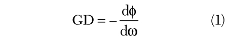
where
dφ = total phase shift
ω = angular frequency
Also, the group delay flatness in the operating frequency band is an important parameter for observing the phase linearity of a receiver system, transmitted signal and so on.

To find the method to control the group delay, it is necessary to analyze a shunt resonance circuit, as shown in Figure 1. The input admittance of the resonance circuit is expressed as

and the transmission characteristic can be expressed as
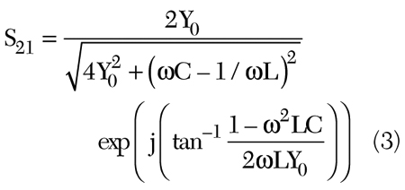
If the particular resonance frequency, ω LC = 1 of the parallel resonator is maintained, the magnitude and the phase coefficient would be kept constant. Then GD, the differential phase component of the transmission coefficient with respect to the angular frequency, can be derived from Equation 4 at the particular resonance frequency, by using Equations 1 and 3.
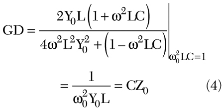
From Equation 4, the group delay time increases proportionally to the capacitance. On the contrary, as the inductance increases, the group delay time decreases, proving the inverse proportionality to the inductance. Keeping the resonant frequency fixed, the group delay time can be adjusted by several combinations of a capacitance and an inductance.
Implementation and Measurement of the GDTA
Varactor Diode Measurement
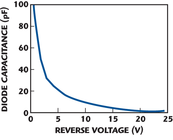
A varactor diode is a semiconductor device that is widely used in many applications where a variable capacitance is required. The operation of the varactor diode is based on the fact that a reverse biased PN junction acts as a variable capacitor. The diode capacitance versus reverse voltage of the Sony 1T362 device used has a variation of approximately 2.3 to 100 pF, as shown in Figure 2.
Variable Equivalent Inductor and the GDTA Unit
There are few variable inductors in microwave devices. Even though there is an active inductor using a gyrator structure that can change the inductance, the quality factor (Q) is not high enough and changes according to the control voltage.9,10 For that reason, the active inductor is not yet widely used. The series combination of a lumped inductor and varactor diode can be used as a variable equivalent inductor. Since it is difficult to fabricate high Q inductors with a small tolerance, however, the combination of varactor diode and lumped inductor is not suitable. A transmission line of characteristic impedance Z0, terminated with a varactor, can also be used as a variable inductor, as shown in Figure 3. A transmission line characteristic shifts from capacitive to inductive, as shown in Figure 4. However, the physical length of a transmission line is too long in case of a low operating frequency.

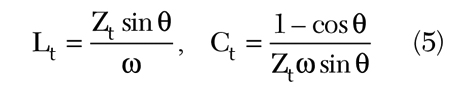
In this work, a high impedance transmission line, terminated with a varactor, is used to implement the variable inductor. Figure 5 shows the lumped element equivalent circuit of the transmission line, where Zt and θ are the characteristic impedance and electrical length of the tramission line, respectively. The values of the equivalent lumped elements are
Using the varactor diode and the proposed variable equivalent inductor, the GDTA unit shown in Figure 6 was designed. The varactor diode is operated as the variable capacitor, and the high impedance transmission line terminated with the varactor diode is operated as the variable equivalent inductor.

The transformation procedure of the variable equivalent inductor is depicted in Figure 7. The capacitor C1 denotes the variable capacitance and C2 is used for the variable equivalent inductor with the high impedance transmission line, respectively. The high impedance transmission line was replaced with the lumped element equivalent circuit. Since C2 shares node A with Ct, and C1 shares node B with Ct, these pairs of capacitors can be substituted with C' and C2+ Ct. Finally, C1+ Ct can be represented as C'' and the series connection of Lt and C' can be substituted with L'. Equation 6 shows the equivalent reactance of the transmission line terminated with the varactor diode. As long as the equivalent reactance (XL) is positive, it has an inductive characteristic. Therefore, as C' is varied, a variable inductance can be obtained.
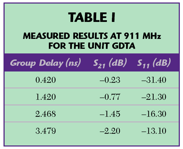

The values of the variable capacitor and inductor are controlled by two separate bias voltages that must satisfy the fixed resonance condition. The measured results of the proposed GDTA unit, tested at 911 MHz, are shown in Table 1. As GD is increased, the reflection characteristics are getting increasingly worse, due to the parasitic component of the varactor diode.

The Balanced GDTA
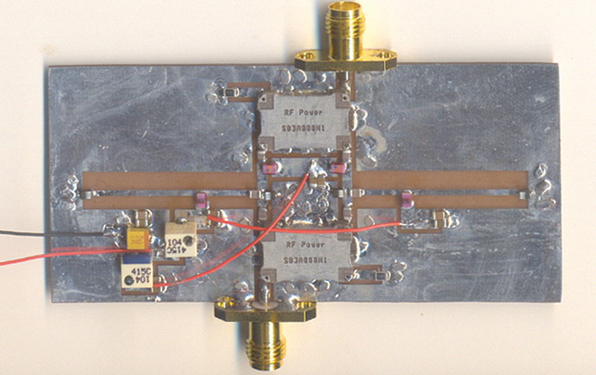
In order to obtain better reflection characteristics of the GDTA, a balanced GDTA structure is proposed and shown in Figure 8. It is composed of two hybrid couplers (RF Power, S03A888N1) and two unit GDTAs. The overall circuit size is 79 x 39 mm, as shown in Figure 9. The implemented GDTA was tested in the Korean RFID frequency band (908.5 to 914.0 MHz). The group delay measurements of the proposed balanced GDTA are shown in Table 2 and Figure 10.
Although a group delay time variance greater than 3 ns could be obtained, the transmission and the group delay time flatness in the high group delay time region are in a trade-off relationship, so that there was no choice but to limit the actual variation range to 3 ns. In that case, the magnitude flatness is less than 0.1 dB in the pass band and the maximum reflection coefficient is approximately –24.4 dB. These satisfactory results can be applied to systems where the group delay time matching with good flatness is critical.
Base Station FFW PA Design Using the Proposed GDTA
To obtain broadband signal cancellation, broadband amplitude, out-of-phase and group delay matching are essential, and must be matched simultaneously. Due to the fact that the conventional signal canceller cannot satisfy the out-of-phase and equal group delay matching at the same time inherently, an equal group delay signal canceller has been proposed.11

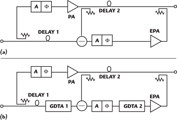
To prove the validity of the proposed GDTA, an FFW PA for the digital cellular band using a balanced GDTA and equal group delay signal canceller was implemented. The performance of the implemented linearization system with a commercial power amplifier of 120 W PEP for base station use was measured. Figure 11 shows the block diagrams of the conventional FFW PA and of the proposed FFW PA using the GDTA and the equal group delay signal canceller. GDTA 1 is put between the delay 1 and signal canceller, and GDTA 2 is inserted in front of the error power amplifier (EPA). Usually, the group delay matching is a time-consuming process and requires much effort to obtain wideband signal cancellation. One of the several advantages of the GDTA is that the group delay time matching is much easier to achieve by just adjusting the control voltages.
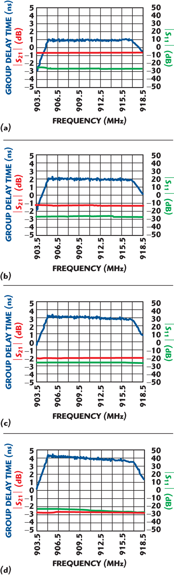
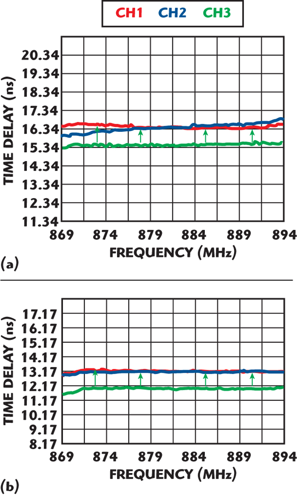
Figure 12 shows the group delay time matching process of the carrier cancellation loop and IMD cancellation loop. After finishing the coarse tuning using a coaxial cable, the fine-tuning is done very easily with simple voltage controls. The blue lines are the amount of the time delay of the main and error amplifier path, and the green and red lines represent the time delay before and after the fine-tuning, respectively. The mismatch of the carrier cancellation loop is due to the poor group delay flatness of the main amplifier.
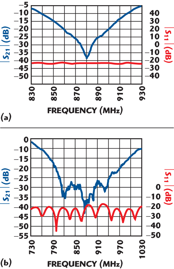
Figure 13 shows the signal cancellation loop suppression results, using the proposed GDTA, measured with a network analyzer. The proposed canceller cancels the input signal by more than 23 dB from 869 to 894 MHz. The IMD cancellation characteristic using the proposed GDTA is also shown. The input signal is cancelled by more than 30 dB within 880 ±50 MHz. The frequency bandwidth, in which the signal is cancelled more than 20 dB, is greater than 160 MHz.
For experimental verification, the output power spectral density of the FFW PA was measured with and without the FFW loop, using a forward-link CDMA IS-95A four-carrier signal for the digital cellular band. These measurement results are shown in Figure 14. The ACLRs at 3.125 and 4.375 MHz offset are shown through the output dynamic range, and the measured power spectral density of the implemented FFW PA at an average output power of 40 dBm is shown before and after cancellation. The ACLR at a 3.125 MHz offset is –52.12 dBc, improved by approximately 17.2 dB by the cancellation. The amount of improvement is smaller than expected from the results shown on the network analyzer because of the limitation of the measurement setup. The proposed system shows excellent linearity throughout the output dynamic range.
Conclusion
A new GDTA unit was designed that can control the group delay time of a signal using a parallel resonance circuit. Keeping the resonance frequency fixed, the group delay time can be adjusted by the combination of values of capacitance and inductance through a simple voltage control. The fabricated balanced GDTA improves the poor reflection characteristics of the single GDTA unit and offers a group delay time variation of approximately 3 ns. Also, the validity of the proposed GDTA was established by applying the circuit to a feedforward linearization. The proposed GDTA will contribute not only to the improvement of the quality of a communication, but also to the simplification of the group delay time tuning procedure of a communication system.
Acknowledgment
This article was partially supported by the CBNU fund for overseas research, 2006 (OR-2006-4).
References
1. S.C. Cripps, Advanced Techniques in RF Power Amplifier Design, Artech House Inc., Norwood, MA, 2002.
2. P.B. Kenington, R.J. Wilkinson and J.D. Marvill, “Power Amplification Techniques for a Linear TDMA Base Station,” 2002 IEEE Global Telecommunication Conference Digest, Vol. 1, pp. 74–78.
3. F.H. Raab, P. Asbeck, S.C. Cripps, P.B. Kennington, Z.B. Popovic, N. Pothecary, J.F. Sevic and N.O. Sokal, “Power Amplifiers and Transmitter for RF and Microwave,” IEEE Transactions on Microwave Theory and Techniques, Vol. 50, No. 3, March 2002, pp. 814–826.
4. W.T. Kang, I.S. Chang and M.S. Kang, “Reflection-type Low Phase-shift Attenuator,” IEEE Transactions on Microwave Theory and Techniques, Vol. 46, No. 7, July 1998, pp. 1019–1021.
5. S.J. Kim, J.Y. Lee, J.C. Lee, J.H. Kim, B. Lee and N.Y. Kim, “Adaptive Feedback Interference Cancellation System (AF-ICS),” 2003 IEEE MTT-S International Microwave Symposium Digest, Vol. 1, pp. 627–630.
6. T. O’Sullivan, R.A. York, B. Noren and P.M. Asbeck, “Adaptive Duplexer Implemented Using Single-path and Multi-path Feedforward Techniques with BST Phase Shifters,” IEEE Transactions on Microwave Theory and Techniques, Vol. 53, No. 1, January 2005, pp. 106–114.
7. I. Bahl and P. Bhartia, Microwave Solid Circuit Design, John Wiley & Sons Inc., New York, NY, 1988, pp. 626–659.
8. D.M. Pozar, Microwave Engineering, Second Edition, John Wiley & Sons Inc., New York, NY, 1998.
9. R. Mukhopadhyay, Y. Park, P. Sen, N. Srirattana, J.S. Lee, S. Nuttinck, A.J. Joseph, J.D. Cressler and J. Laskar, “Reconfigurable RFICs for Frequency-agile VCOs in Si-based Technology for Multi-standard Applications,” 2004 IEEE MTT-S International Microwave Symposium Digest, Vol. 3, pp. 1489–1492.
10. S.J. Seo, N.S. Ryu, H.J. Choi and Y.C. Jeong, “Novel High-Q Inductor Using Active Inductor Structure and Feedback Parallel Resonance Circuit,” IEEE RFIC Symposium Digest, 2007.
11. Y.C. Jeong, D. Ahn, C.D. Kim and I.S. Chang, “Feedforward Amplifier Using Equal Group Delay Signal Canceller,” 2006 IEEE MTT-S International Microwave Symposium Digest, pp. 1530–1533.
Heungjae Choi received his BS and MS degrees in electronic engineering from Chonbuk National University, Jeonju, Korea, in 2004 and 2006, respectively. He is currently working toward his PhD degree. His research interests include broadband linearization and high-efficiency RF PAs.

Yongchae Jeong received his BS, MS and PhD degrees in electronic engineering from Sogang University, Seoul, Korea, in 1989, 1991 and 1996, respectively. From 1991 to 1998, he was a senior engineer in the information and communication division of Samsung Electronics. Since 1998, he has been in the division of electronics and information engineering at the Integrated Circuit Design Education Center of Chonbuk National University, Jeonju, Korea. He is currently an associate professor teaching and conducting research in the areas of microwave devices, base station amplifiers, linearization technology and RFIC design.
J. Stevenson Kenney received his BSEE, MSEE and PhD degrees in electrical engineering from the Georgia Institute of Technology in 1985, 1990 and 1994, respectively. He has over 14 years of industrial experience in wireless communications. He has held engineering and management positions at Electromagnetic Sciences, Scientific Atlanta, Pacific Monolithics and Spectrian. In January 2000, he returned to Georgia Tech as an associate professor in electrical and computer engineering. His research interests include acoustics, microsystems and microwave design.
Chul Dong Kim received his BS degree in electronic engineering from Seoul National University, Seoul, Korea, in 1971, and his PhD degree from the University of Wisconsin, Madison, in 1985. He is currently president and chief executive officer (CEO) of Sewon Teletec Inc., Kyungki, Korea, a company specializing in RF PAs.