
As the complexity of these electronic products intensifies, constraining EM emissions within dense printed circuit boards (PCB), IC packages and even the IC itself requires careful engineering. With package pin counts in excess of 5000 and ever-smaller pitch spacing compressed into shrinking board space, the potential for electromagnetic interference is greatly increased.
To meet both manufacturer’s specifications and engineers’ requirements for signal integrity, cross-talk and EMI compliance, designers must be able to identify and constrain critical high-speed signals at all stages of the design process.
With space and functionality at a premium, engineers may be forced to reduce or eliminate enclosure-level shielding vis-à-vis enhanced circuit segregation and noise suppression. At the same time, improving time-to-market and compliance costs will require a reduction in the number of design iterations. Achieving these goals requires the application of design best practices, EM/circuit co-simulation and early EMI/EMC test verification. By treating EMC as a design issue rather than a test and measurement issue, design teams will ultimately save development time. This article examines the challenges associated with EMC performance and some of the design rules being implemented.
Addressing EMC at the Early Planning Stages
Electromagnetic waves, conduction and inductive/capacitive coupling are all sources of EMI. Excessive emissions leading to EMC failure can be related to poor component shielding, enclosure design and/or cabling, which can couple energy from inside the system to the outside world. A harmonic signal from a seemingly harmless low-amplitude clock may be at the right frequency to excite a resonance within a module or housing, resulting in elevated currents that will radiate through an aperture (dimension dependent) or cable. System-level EMC design must therefore adequately model the chassis, any venting/seams and cabling in addition to the PCB.
Designing for EMC at the system level should initially focus on defining and segregating functional blocks into high-speed, noisy, aggressor circuits, and sensitive, quiet, victim circuits. The likelihood of a circuit node being aggressive depends on its maximum dV/dt and/or dI/dt. The likelihood of a circuit node being a victim of EM phenomena depends on its signal levels and noise margins. Noisy components include clock generators, micro-controllers, switch-mode power transistors, rectifiers, heatsinks, etc. These noisy components should be somewhat isolated from sensitive ones such as analog ICs. Since EMI must reach the conductors in order to disturb the components, any conducting loops, long length and large surface areas are vulnerable to EMI. This vulnerability makes the PCB itself a leading target for EMC improvements. Decreasing noise source emissions, weakening the capacity of noise carriers and increasing the immunity to EMI in the most susceptible areas of the PCB are among the most effective ways to improve EMC performance.
Some common practices for improving EMC performance on the PCB include:
- Placement of decoupling capacitors between power and ground on packages and printed circuits boards where voltage fluctuations are determined to exist. Multiple caps should be used in parallel depending on the frequency of the IC in consideration. Capacitors should be selected based on its self-resonant frequency (SRF).
- Use of ferrites for decoupling power planes from power pins.
- Power planes should be backed off from the edge of the board.
- Adequate termination of all high-frequency clock lines.
- Connectors need to be properly filtered.
- Use of stitching vias at the board edges.
- Tightly coupled forward and return path currents for critical nets.
To address EMC issues, PCB floor planning begins with a focus on circuit segregation followed by consideration for any shielding and filtering techniques that will need to be physically implemented. Layout of the mechanical assembly and physical component placement should come early in the product development lifecycle. As the density of electrical components increases and switching speeds move into the gigahertz range, tried and true techniques are less likely to be successful. Design teams may find it is faster to investigate the electrical behavior of individual structures at the new higher frequencies and establish a set of acceptable geometric guidelines for interconnects then troubleshoot a fully assembled yet non-compliant system.
Component-to-component interaction will still necessitate system-level testing and/or simulation. Since design layouts are generated using two-dimensional CAD, it is not uncommon to inadvertently create a final assembly with a very sensitive circuit in close proximity to a noisy circuit. The resulting signal quality problems may lead to EMC failure. To avoid troublesome EMI issues design teams should apply three-dimensional EM analysis to proposed final assembly drawings in order to verify proper behavior.
PCB Materials
Relative to epoxy-glass substrates such as FR4, homogeneous substrates including teflon, pure polymers and liquid crystal polymer (LCP) generally offer a lower dielectric constant (k) and loss tangent. The lower k leads to a higher propagation velocity, while the lower losses benefit the transmission of high frequency signals over longer distances.
Low-k substrates can be employed to benefit EMC. Higher impedance transmission lines lower the currents flowing in them, thereby reducing their emissions. Higher impedance lines are created from thinner traces, which for thin substrate layers may require a trace width too small for low-cost manufacture. Lower-k dielectrics use wider traces for the same characteristic impedance, making it easier or less costly to use higher impedance transmission lines, thus reducing currents and lowering emissions. Of course, proper impedance matching between components is required to minimize standing waves.
The use of low-k substrates has been commonplace in microwave applications such as satellite communications. As signal speeds increase, the EMC benefits of using low-k substrates would seem to favor their use in more mainstream PCBs, particularly PC motherboards and cellphones. However, many RF engineers have been able to devise designs that allow the continued use of low-cost FR4 and similar materials. When signals are 10Gb/s or more, traces on glass-fibre substrates like FR4 that exceed 600mm in length will have serious signal integrity and/or EMC difficulties.1
PCB Design Considerations
Some of the specific areas of PCB design that ultimately improve the overall EMC performance of the PCB include:
- Reduction of inter-layer noise.
- Optimization of the impedance between power and ground reference planes.
- Minimization of transmission line cross-talk and reflections.
- Improvements to the simultaneous switching output (SSO) response.
- Alleviation of edge radiation.
Controlling the EM environment for a single PCB is easier than addressing the EM compatibility between multiple PCBs interconnected by wires and cables. The preferred, cost-effective way to meet EMC requirements is to use a single multi-layer PCB with separate layers dedicated to the ground and other layers for the power supply, resulting in good decoupling and shielding effects. When economical requirements prohibit the use of this type of board it becomes even more critical to pay special attention to the quality of the high-speed interconnect structures as well as the construction and location of the ground and power supply planes.2
It is a common practice to include individual distribution of a 0 V reference plane to every block with a single point for gathering all returns. Loops should be avoided wherever possible or should at least have a minimum surface area. Because supply loops can act as an antenna, both emitting and receiving EMI, the power supply should be implemented close to the ground line and its surface area minimized. The location of power planes should be optimized and backed off from the edge of the board to reduce edge coupling. Filling all component-free surfaces of the PCB with additional grounding is a commonly used way to create additional shielding. As a safeguard, designers should apply EM simulation to these structures and look for unexpected resonances before physical prototypes are manufactured.
The noise between the power and ground planes of the structure is known as interlayer noise. It is possible to simulate this noise by exciting the region between the planes with a Gaussian source or pulse. The pulse propagates from the source location to the edge of the board and is reflected. Over a period of time, the peak noise or voltage at each location between power and ground can be plotted and visualized. It is possible to see, for example, that the voltage is markedly lower where decoupling caps or shorting vias are located.
All PCB connectors carrying power and ground should use adjacent pins. For long connectors, a number of power/ground pin pairs should be spread along its whole length. For wide connectors, the power/ground pin pairs should be spread across the entire area, space permitting. Ideally there should be a power/ground pair adjacent to each signal pin or at least adjacent to critical interconnects carrying Gb/s signals. The use of differential pairs for high-speed channels relaxes this constraint to one power/ground pair for every two or more signals.3
PCBs and System-level EMC Design
The worldwide printed circuit board market is driven by applications of wireless, communications and computing. Modern PCBs include mixed-signal functions with RF, digital, data conversion and high-performance digital signal processing (DSP). It is critical to be able to design such complex boards while maintaining signal integrity, power integrity and EMI/EMC performance. New simulation tools make it possible to combine board-level electromagnetic simulation with advanced circuit simulation to accurately predict PCB performance. Currents and voltages resulting from circuit-level simulations can then be applied within a full 3D EM field solver to predict EMC radiated emissions.
In an ADSL modem, for instance, there are challenges of the complexity of the mixed-signal design combined with the requirements for successful EMC compliance. The electromagnetic simulator from Ansoft called Siwave™ can read standard Cadence and Mentor board files and then compute full-wave fields, S-parameters and radiation. Using such a tool allows engineers the ability to locate and modify radiation sources. By coupling to a nonlinear circuit simulator, true nonlinear models for sources and loads on various circuit nodes can be computed. Frequency-dependent IBIS and SPICE circuits couple with the S-parameters to provide an accurate representation of the frequency-dependent voltages and currents within the PCB. Sources such as power and ground planes, clock traces, data traces and memory interfaces commonly produce electromagnetic radiation. Radiation from these sources can be computed in the near-field, at three meters, and in the far-field.
The above outlined procedure was followed to predict radiation emanating from an ADSL modem PCB. The initial design of that modem board provided excellent performance; however, an expensive shielding box over critical components was required to meet EMC compliance. The goal of this work was to redesign the PCB so that the shield was no longer necessary.
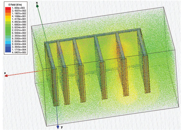
Seven such modem PCBs were then placed on a backplane chassis for evaluation in a true 3D environment. A model in the 3D full-wave solver (in this case Ansoft’s HFSS™) uses the SIwave circuit plus board-level simulation results as the source for secondary radiation computation in HFSS. Invoking the equivalence principle,4 electromagnetic fields computed by SIwave are placed on surfaces surrounding the individual PCBs in the HFSS model. HFSS then computes 3D radiated fields for the entire system containing the seven ADSL modem boards plus backplane chassis.
Figure 1 shows a plot of the electric near-fields surrounding the PCBs in a 3D “fog” plot. The density and color of the fog is mapped to the intensity of the electric field. Various hot spots between PCBs can be identified easily by observing this field plot.
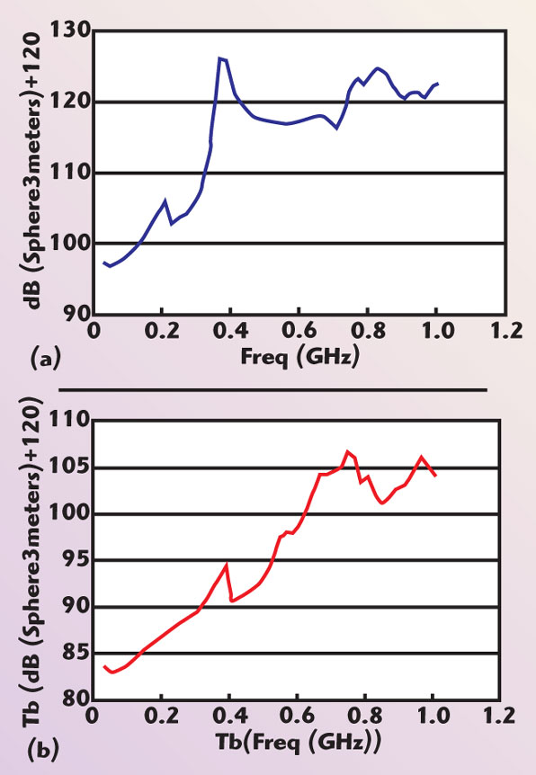
Figure 2a is a plot of the radiated fields at three meters versus frequency for the initial PCBs without the shield. A maximum radiation of 126 dB microvolts/meter occurs near 375 MHz.
Figure 2b is a similar plot; however, design modifications to the PCBs, including impedance control, power/ground plane decoupling for power integrity and certain trace re-routing were included in a new design.
As can be seen in the figure, the radiation at all frequencies was reduced dramatically. Near 375 MHz, the new design produced 94.5 dB microvolts/meter, a reduction of over 31 dB.
Maximum radiation of 106.5 dB microvolts/meter was pushed up to the higher 750 MHz frequency.5
Figure 3 summarizes a design flow based on coupled 3D electromagnetic plus circuit simulation and design for EMC compliance. Individual board-level simulations are performed using the 3D planar tool.
Design rules can be developed so that engineers can design with EMC compliance in mind. Modifications to the layout design for signal integrity, power integrity and trace routing are made and simulations allow engineers to understand the effect on EMC.
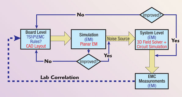
Results from individual board simulations become the noise source for simulations of full 3D system simulations of boards placed in a backplane and chassis. Redesign at all levels can be performed prior to PCB fabrication. Finally, verification of the final design can be made for EMC by lab measurements.
Shields and Module Enclosures
Shielding, filtering and isolation techniques may be required to reduce the radiated and/or conducted EMI across segregated areas of the design down to acceptable levels. Selecting the most cost-effective methods for shielding each interface will depend on the given operational EM environment, the emissions/immunity characteristics of the circuits concerned, and the cost and size requirements. Connections to the outside world may need the full range of suppression techniques, including shielding, filters, isolating transformers and electrostatic discharge (ESD). Shielding may be applied to chips or areas of the PCB, the whole PCB, subassemblies of PCBs, entire assemblies of PCBs or the entire product.6 Since radiation leakage from the PCB will almost always be minimized using shielding, the coupling between the PCB and the shield should be examined using 3D analysis.
Microwave absorbent material can be used to effectively dampen undesired cavity resonances by attenuating or absorbing high frequency energy. Microwave absorbers designed for damping cavity resonance are most often made from high-permeability materials with broad frequency magnetic loss (permeability) properties. They are usually available in thin elastomer sheets ranging in thickness from 0.010 inch (0.25 mm) to 0.040 inch (1.02 mm) that can be cut and formed to fit the conductive inside surface of the enclosure.
It is nearly impossible to eradicate all electromagnetic fields in the board design. Connections to the board and wires carrying RF currents in and out of the system will have electromagnetic fields associated with them. The conducted RF currents carrying the so-called “common mode” currents are often the most significant contributors to the electromagnetic emissions. Additional consideration should be paid to the shield or enclosure itself. If the wavelength is similar to the dimensions of any vents, seams or slot apertures, resonance will occur and electromagnetic fields will be efficiently radiated out. Shielding that relies on contact between extended surfaces is especially prone to EMI problems due to the formation of gaps. Intentionally designing irregularly spaced gaps into the shielding will minimize this problem and avoid the creation of a periodic resonating structure.
Analyzing Enclosures, Seams and Vents
Thorough analysis of the radiation from the PCB to other components in a system and the requirements/effectiveness of an enclosure or shield will require either a dedicated measurement system or 3D simulation tools such as MicroStripes from Flomerics, Microwave Studio from CST or HFSS from Ansoft. At the system level, today’s 3D solvers use detailed internal structures to accurately capture the system resonances.

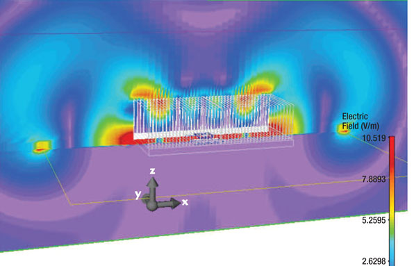
Visualization of fields, currents and radiation patterns allows problem frequencies and emission sources to be readily found, including important details concerning the effects of seams, gaskets, cables and filtering on EMC. For example, MicroStripes and measurements were used in the analysis of a PC chassis (see Figure 4).
At the circuit board level, MicroStripes analyzed the field and current distributions within a module in order to identify EMI ‘hot-spots’ and resonances as well as the effects of component placement on related emissions and immunity.
These studies can also be extended to cables and wires to investigate cable routing and filtering.
In the full system-level PC model, the electric and magnetic fields were sampled both inside the enclosure and at points 3 m away.
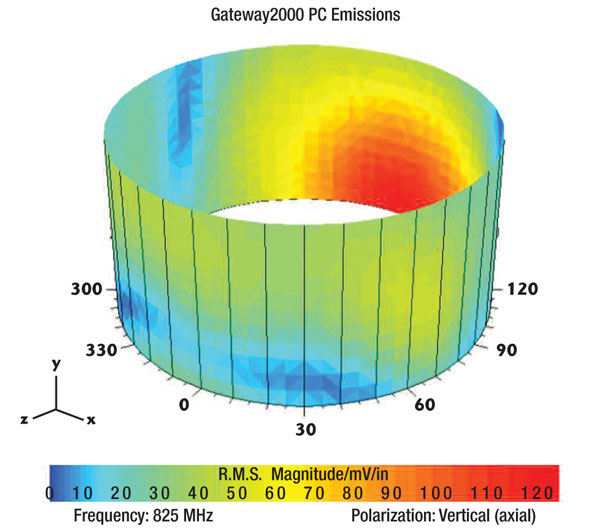
The radiated electric field at 3 m in front, behind and to the sides of the PC displayed in Figure 5 shows radiation peaks at 133, 390, 825 and 900 MHz.
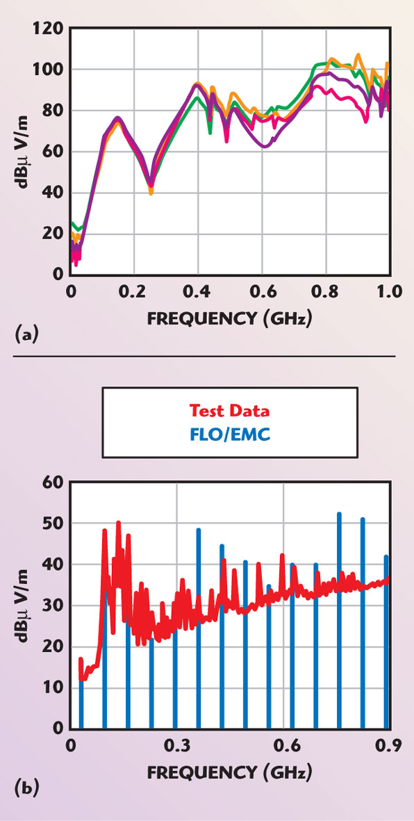
This impulse spectrum reveals the continuous broadband response of the PC. The actual PC generates discrete frequencies based on the fundamental clock frequency and its harmonics as shown. To validate the viability of this analysis, the specifications of this older, relatively slow processor were determined to be a 66 MHz bus clock and 0.15 to 1.5 ns rise/fall times based on the manufacturer’s development guide.
Near-field probing and visual inspection of the crystals revealed fundamental clock frequencies at 20, 24.3 and 33 MHz. The simulation plot in Figure 5b was obtained by multiplying the MicroStripes impulse spectrum by the spectrum of a 33 MHz clock with a 1ns rise/fall time.
The numerical results are compared with the test data taken in an anechoic chamber performed by Curtis-Strauss Compliance laboratories.
Notice that the system is virtually within FCC Class B limits, even with the reset wire unshielded. In the MicroStripes simulation the chassis seam was treated as worst case or completely open exaggerating the emissions above 700 MHz.
The EMC analysis also provides a cylindrical scan around the system on a 3M radius, mimicking the FCC EMC test configuration. The high radiation behind the PC, shown in Figure 6, indicates that the radiation is vertically polarized, suggesting that the seams are responsible.7
An alternative time domain 3D EM simulator, Microwave Studio (MWS) from CST, can also be used for EMC/EMI analysis.
The MWS software is based on a finite integration technique (FIT) solver, which provides direct transient analysis of typical interference signals from periodic and nonperiodic pulses, electrostatic discharge (ESD), lightning and nuclear electromagnetic pulse (LEMP, NEMP).
Time domain EM simulators are well-suited for electrically large models and large bandwidth models wherein a single simulation excites a broad range of frequencies in the time domain.7
The hexahedral mesh in conjunction with the perfect boundary approximation (PBA) and thin sheet technique (TST) avoids the use of a very fine mesh to accurately model slots and gaps located on the enclosure (see Figure 7).
Similar to the frequency domain code, MWS can be used by engineers to study an enclosure’s shielding effectiveness (SE) by monitoring the field strengths inside an enclosure with respect to an external plane wave illumination (EMC) or the field strength outside an enclosure with respect to a radiating source inside the enclosure (EMI).9

For example, Figure 8 illustrates the SE evaluated by means of CST Microwave Studio for a rectangular box of size (30 X 12 X 30 centimeters) with a rectangular aperture of size (10 X 0.5) located at the center of the frontal wall. Excellent agreement can be observed when comparing the computed data with measured results as well as with other numerical techniques.
IC Level Concerns
The IC design challenges for EMI reduction include high-speed inductance effects, coupling due to high bus complexity as well as package parasitics.
EMI is often addressed by modification to the PCB components, the IC I/O design or both. When the silicon is in closer proximity to the 0 V plane in the PCB, the EMC performance is generally enhanced. This is a benefit shared by chip-scale packages (CSP) and chip-on-board assemblies (COB).
For both types of IC packaging, the internal interconnects are smaller, thereby reducing their effectiveness as antennas. Chip-on-board construction also allows conductive ink shielding to be printed directly over its “blob top” epoxy resin or silicone shell for greater EMI protection.

Many integrated circuits and power semiconductors require a heatsink for thermal dissipation. Unfortunately, the stray capacitance between the IC and a metal heatsink gives rise to noise currents in the heatsink when the IC voltage fluctuates.
Electric fields from the heatsinks can cause radiated emission or conducted emissions if they are coupled to a conductor.
Connecting the heatsink to the reference voltage of the IC that is the source of the voltage fluctuation will improve the EMC behavior. Resonance effects for a heatsink occur when the dimension of the heatsink or the cavity(ies) it creates exceeds λ/10 at the highest frequency of concern.
When a signal frequency or its harmonic coincides with a resonant frequency, emissions from can increase by 30 dB or more (see Figure 9).10
Conclusion
As the demand for more functionality, in reduced-scale components leads to the crowding of high-frequency signals in tight spaces, the potential for EM interference is greatly increased. Coupled with the pressure to reduce design iterations, implement cost-effective EMC solutions and be first-to-market, engineering teams need to consider EMC through all stages of design. To resolve EMI issues expeditiously, engineers should turn to the growing wealth of EMC knowledge currently available in literature and on the web. EM simulation tools also play a critical role allowing EMC/EMI engineers to be more methodical in their approach to exposing potential problems and avoiding a costly re-spin.
References
- K. Armstrong, “Design Techniques for EMC & Signal Integrity—PCB Design and Layout,” UK EMC Journal, Jan.–Dec. 1999.
- K. Armstrong, “Advanced PCB Design and Layout for EMC,” EMC & Compliance Journal, March 2004, available from http://www.compliance-club.com.
- Ibid.
- C. Balanis, Advanced Engineering Electromagnetics, John Wiley & Sons Inc., New York, 1989, p. 329.
- L. Williams, “Complex EMI/EMC System Design,” Ansoft Application Note, April 2007.
- K. Armstrong, Advance PCB Design.
- D.P. Johns, A. Francois-Saint-Cyr and F. German, “EMC & Thermal Design Conflicts in a Pentium PC,” Flomerics Application Note, July 2002.
- J. Reed, notes from IEEE EMC Phoenix, December 6, 2006, available on-line (http://www.ewh.ieee.org/r6/phoenix/phoenixemc/previous.htm).
- CST, “Test of EMC-radiation Norms,” application note available on-line (http://www.cst-america. com/Content/Applications/Article/Test+of+EMC-Radiation+ Norms).
- D.P. Johns, “Taking the Guesswork out of EMC/EMI Design,” Flomerics Web Presentation, October 2005.