
IEEE 802.16e mobile WiMAX is currently being developed as the next-generation communication standard competing with wireless local area network (WLAN), code division multiple access (CDMA), evolution data optimized (EVDO), enhanced data rates for GSM evolution (EDGE) and high speed downlink packet access (HSDPA), even though early applications for mobile WiMAX technology will be limited to high data rate communication purposes. This article discusses the key mobile WiMAX 802.16e radio frequency (RF) receiver requirements including NF, P1dB, IP2, IP3, and dc settling time to be able to identify RF system requirements. System simulations such as utilizing matlab software to extract EVM in different conditions including pilot tracking loop, will also be described to illustrate its effect with high-data rate mobile WiMAX system design.
Overview of 802.16e OFDMA Mobile WiMAX
IEEE 802.16e mobile WiMAX is currently being developed as a next generation communication standard competing with WLAN, CDMA, EVDO, EDGE and HSDPA even though early application for mobile WiMAX technology will be limited to high-data rate communication purposes. However, eventually these technologies will be competing with each other with various applications. IEEE 802.16e specifically targets mobility from previous IEEE 802.16 standards as it can be indicated from the standard [1]. Orthogonal frequency division multiplexing (OFDM) is a multi-carrier modulation technique that transmits data over a number of orthogonal sub-carriers, which consist of data and pilot within various formats of frame structures.
Simple OFDM signal formats and sub-carriers in frequency domain are shown in equation 1, figure 1 
Where,
Ck = a complex number, the data to be transmitted on the sub-carrier whose frequency offset index is k, during the subject OFDMA symbol Nused = Number of used sub-carriers (which include DC sub-carrier)
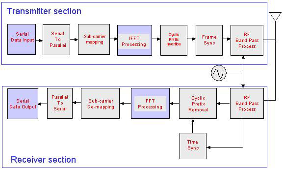
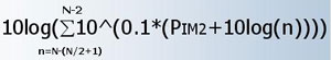
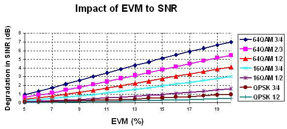
Tg = guard time Pilot assignment and number of sub-carriers are variables of permutation formula and bandwidth of the signal and modes. In addition, guard sub-carriers are suppressed for the frequency shaping. Fig. 2 shows an OFDMA frame structure in time division duplex (TDD) mode. The preamble is for the frequency synchronization and compensation of amplitude as well as phase of signal. Down, uplink bursts are mapped to two dimensions which are time and sub-channel. There are TTG, RTG which are time gap between transmit and receive, and more detailed definition will be presented in later dc settling requirements. Now we are going to look at actual transmitter and receiver structures with OFDM modulation in Fig. 3. The serial data input is mapped to fast fourier transform (FFT) bins that are assigned and an inverse FFT (IFFT) process is carried on as a modulation method. A cyclic prefix is inserted to mitigate multi-path fading and inter symbol interference, sacrificing an increase in bandwidth. At the final stage, there is an RF band pass process, which shifts baseband signals to a carrier frequency. At the receiver side, a reverse process is performed to extract actual original data. The minimum sensitivity, RSS from 802.16e standard is as shown below RSS = – 114+ SNRRx–10×log10(R) +10×log10 ((FS ×Nused)/NFFT) + ImpLoss + NF Where, SNRRX = receiver SNR The required minimum sensitivity level, RSS was calculated for the different modes such as QPSK, 16QAM, 64QAM with various coding rates in Table 1, 2, and 3 as shown below. The assumptions here are repetition factor, R is not considered and Nused is based on PUSC for the worst case. As we can see from the required RSS, implementation loss (ImpLoss) and noise figure (NF) are the ones that we need to decide for the target performance in the system. Dynamic range of system is defined as the ratio of the maximum input signal level that the system can handle and minimum input signal level that the system can process the signal. Therefore IEEE 802.16e mobile WiMAX has a dynamic range requirement as listed below. -104 – (-30)=74dB Where, -104 = the minimum sensitivity level on the device -30 = maximum signal level defined in the standard Since the maximum signal level will be –30dBm at the device input, the system needs margin from this level to prevent any distortion components that can degrade system performance. This margin can be set based on AWGN 0.1 percent peak to an average power ratio point which corresponds to –37dBc error vector magnitude (EVM). The -18dBm P1dB requirement can be set as explained below. -30 + 12 = -18dBm Where, -30dBm = maximum signal level 12dB = AWGN 0.1% peak to average point Input system IP2 requirements can be derived from specified non-adjacent orthogonal frequency division multiple access (OFDMA) signal test conditions since non-adjacent signal power is higher than adjacent-signals in the standard. The IEEE 802.16e standard specified adjacent, non- adjacent test conditions are shown below. 16QAM 3/4: adjacent channel power is 11dB higher than signal The system has to keep the sensitivity level 3dB below the minimum threshold with these adjacent, non-adjacent signals. The inband IM2 product with dc null from the non-adjacent signal can be calculated from equation below (2): Where, PIM2 = IM2 product of two sub-carrier input case N = number of sub-carriers Sum of n = number of total inband IM2 product A summary of the required system input IP2 is presented in table 4. The assumptions made for the IP2 analysis include: A target radio noise figure of 3dB Radio error vector magnitude (EVM) of 8 percent and Implementation loss of 2dB Sufficient amount of filtering of non-adjacent signal in either analog domain or digital domain in FUSC mode. The in-band IM2 product envelope shape is shown in Fig. 4 and is displaying each sub-carrier point even though it appears connected. Therefore the actual in-band power will be scaled from this picture. Input system IP3 requirement is derived from a specified adjacent channel OFDMA signal shown in the IP2 requirements section. The in-band IM3 product with dc null from the adjacent signal can be calculated from the following equation (3): Where, A = total in band IM3 product As we can expect from equation 3, the input system IP3 requirement will be easily achieved to meet the specification. However, mobile devices are becoming more integrated with different standards such as Bluetooth, global systems for mobile communications (GSM), CDMA and radio frequency identification (RFID) -- higher IP3 may be required in the future. Therefore the analysis will also depend on the implementation of different modes, as well as factors such as antenna coupling and distance in real air-field conditions. The IEEE 802.16e standard specified TTG, RTG as below: Basestation transmit/receive transition gap (TTG): A gap between the last sample of the downlink burst and the first sample of the subsequent uplink burst at the antenna port of the basestation in a TDD transceiver. This gap allows time for the basestation to switch from transmit to receive mode A gap between the last sample of the uplink burst and the first sample of the subsequent downlink burst at the antenna port of the basestation in a TDD transceiver. This gap allows time for the basestation to switch from receive to transmit mode Requirements of SSTTG, SSRTG for the all profiles are: This means that using a high-pass filter as a way of dc correction loop will be challenged since high-pass filter requires dc setting time and will cause error vector to signal. This leads to a high-data rate case that requires high SNR (such as 64QAM), which will be greatly affected by this scheme. Therefore a detailed analysis will be needed in data domain in conjunction with preamble, pilot-tracking conditions since preamble has the ability to correct phase, magnitude impairments as well as pilot tracking. Figures 5 and 6 show second order high-pass filter step response and settling time. EVM as a simple but best fit radio impairments analysis tool Overview of EVM Modern digital RF communication systems have common goals in transmitting original digital data onto an RF carrier with the least amount of distortion so that the original signal can be recovered accurately without misinterpreting data that was sent. Since the need for high-data rate communication is a critical focus, we need even better signals that have higher signal-to-noise ratio to demodulate the original high-data rate digital bit streams. But figuring out and quantifying all of RF impairments in a RF system and converting these into a bit error rate (BER) to set the proper RF impairments requirements for the each block is not a trivial task. These impairments are in the different forms such as I/Q mismatch, DC-offset, phase ripple and gain ripple. A common measuring tool of impairments called error vector magnitude (EVM) provides adequate information regarding distortions generated by each block to design and implement RF digital wireless systems. EVM is a measure of the scalar distance between the ideal signal and the measured signal. The difference is called the error vector, which represents a percentage difference of the original signal generally. Conceptual error vector can be drawn easily as shown in Fig. 7. Where, Pm = actual measured signal vector The idea is that any given modulated signals such as BPSK, QPSK, QAM can be brought down to a constellation diagram which has both phase and amplitude information for the signal and compute for the error percentage which can be exchangeable to the signal-to- noise ratio. Why is phase noise important in communication systems? Phase noise is one of the most important impairments of the radio systems since it corrupts the information carried in the phase of the carrier since the LO output is not ideal. There are two different types of corruption occurred by phase noise of LO in the radio systems. The first is from in-band (modulated signal band) phase noise, which directly impacts downconverted and upconverted signals as shown in Fig. 8. Another key aspect of the phase noise specification is with an interferer, which is typically called a blocker as shown Fig. 9. The amount of in-band phase noise can be represented as phase error and eventually contribute as one of the system EVMs. Calculating composite EVM can be a useful way of representing radio performance --- especially in high-data rate communications, which requires high signal-to-noise ratio. Second, phase noise at a certain frequency offset is important when the blocker is present. In a CDMA system, there is a radio standard called single tone jammer specification which requires –101dBm sensitivity with –30dBm CW tone at 900 kHz offset from the center frequency of the modulated signal that is present at the antenna input. In this case, one of the major distortion products is the phase noise at a specified frequency offset which covers signal bandwidth, as well as cross modulation from transmitter leakage. In an OFDMA IEEE802.16e system, we know the in-band phase noise is the main EVM contributor for the sensitivity analysis and since the adjacent signal level is only 11dB higher than the signal level in 16QAM ¾ coding rate, and 4dB higher in 64QAM ¾ coding rate, the EVM contribution will be very small for the required IP2 and IP3 calculations. OFDMA pilot tracking scheme can correct phase errors that occur by phase noise as long as the phase noise variations are much slower than the OFDMA period. OFDMA has pilots that are assigned in the sub-carrier which can be used as means of phase and magnitude correction. Complete Matlab system simulations were done to find pilot-tracking impact to phase noise. Simulation results are shown in Fig. 10. FUSC mode was simulated since it has less pilot assigned in sub-carriers. As you can see from the simulation results, limiting loop bandwidth less than 1/symbol time is critical for phase noise impact improvement as well as limiting inter symbol interference (ISI). The IEEE 802.16e standard does not specify the baseband digital filtering scheme, which makes it challenging to implement the analog channel selection filter without knowing the adjacent, non-adjacent channel rejection from the baseband side. Therefore, the filter design was done under the assumption that signal-to-adjacent, non-adjacent channel power ratio with analog filter is at a minimum 10dB, pass band ripple 0.5dB, and following the baseband digital filter will provide enough rejection at adj, non-adjacent channel. Preamble assignment in sub-channel is expected to correct linear block phase and magnitude impairments, as well as frequency synchronization function. However preamble is not considered to correct any linear filter block EVM in this analysis since this can be varied upon how baseband software is being implemented. Simulation was done as shown in Figures 11 and 12 in frequency domain and table 5 for the comparison between data domain and frequency domain. Here, a data domain analysis was performed through complete system a simulation which compares generated data to demodulated data output through IFFT, FFT and band-pass process for the calculation of EVM with 10MHz signal band. The sixth order chebyshev type I filter was used as one of the many examples to show EVM impact with pilot tracking in FUSC mode as worst case. This was done since FUSC requires steeper rejection with more sub-channel assignments within a given band. In real circuit implementations, odd number order analog filters can be realized easily. EVM optimization was not performed since the purpose of EVM comparison was to find better filter architecture and compare between frequency domain and data domain impact. EVM improvement can be varied by how the pilot is assigned at the edge of the filter pass band since most of the phase distortion is from filter band edge characteristics. The exact simulation can be much more complicated as mobile WiMAX IEEE802.16e uses more flexibility in terms of assigning data and pilot sub-carriers. Analog channel selection filter design can be affected by many factors such as receiver architecture, required rejection with adjacent, non-adjacent signals and EVM requirements. At the same time, preamble sub-channel function accuracy as channel compensation, and the pilot tracking impact also needs to be checked with the baseband software implementation algorithm. However, the delay filter may not be needed to compensate phase error if the impairment from filter section is not as critical with the help of preamble and pilot functions as described above. Composite EVM is an easy, simple and accurate predictor of radio system impairments. This is done without using extensive time and money. Different EVM contributors in the receiver are assumed to be independent and identically distributed as Gaussian random variables. The joint PDF of the sum of these random variables is still Gaussian so that EVM can be modeled as additive noise [7]. Basic impairments of each building block are I/Q gain, phase imbalance, LO phase noise, ADC quantization noise, analog low-pass filter magnitude, and phase, high-pass filter (if used as a dc correction loop). Table 6, shows one example of radio EVM budgeting and Fig.13 shows EVM impact to system signal-to-noise ratio. Fig. 13 illustrates how one can budget what percentage of EVM is targeted for the system design and composite EVM can be broken down to each EVM contributor as we mentioned above. This article describes the key mobile WiMAX IEEE 802.16e RF receiver requirements such as NF, P1dB, IP2, IP3, and dc settling time. Complete system simulations were also performed using matlab software to extract EVM in different conditions including pilot tracking loop for the purpose of high-data rate mobile WiMAX system design. 802.16e Part 16: Air Interface for Fixed and Mobile Broadband Wireless Access Systems. 802.16 Part 16: Air Interface for Fixed Broadband Wireless Access Systems. Mobile WiMAX – Part I: A Technical Overview and Performance Evaluation. Ana Garcia Armada, Miguel Calvo “Phase Noise and Sub-Carrier Spacing Effects on the Performance of an OFDM Communication System” IEEE Communications Letters, vol. 2, NO. 1, January 1998. Behzad Razavi “RF MICTOELECTRONICS”. Steve Hilton “WIMAX Nuts and Bolts”. Bala Ramachandran “HDR Impairment analysis” Skyworks presentation document. [8] Kerry Z. Cai and Pengfei Zhang “The Effects of IP2 Impairment on an 802.11A OFDM Direct Conversion Radio Systems. BPSK - Binary Phase Shift Keying Junhyung Lee (Jun Lee) received his BSEE degree from the Kumoh National Institute of Technology, Gumi, S. Korea. He joined Wide Telecom in 1999 as a RF design engineer and worked on WCDMA, CDMA and WLL mobile phone developments and in 2001, he joined Telson Electronics USA, NJ and worked on CDMA2000 mobile phone developments for the U.S. market. In 2004, he joined Skyworks Solutions, Inc. in Irvine, CA where he has been working on CDMA2000, EVDO, WiMAX RF systems and applications and designed CDMA and EVDO single package radio (SPR) solutions. He currently works on WCDMA synthesizer module circuits and system developments for base station applications as a senior systems engineer. His research interests include RF systems, circuits, communication theory and simulations. He is pursuing an MSEE degree from California State University in Long Beach.
Ts = OFDMA symbol duration including guard time
Tf = sub-carrier frequency spacing
t = time (0
Minimum Sensitivity Level
R = repetition factor
FS = sampling frequency in MHz
Nused = number of used carriers
NFFT = number of FFT size used
ImpLoss = implementation loss, which includes non-ideal receiver effects such as channel estimation errors, tracking errors, quantization errors, and phase noise. The assumed values is 5dBNF – noise figure of system
![]()
![]()
Minimum System Dynamic Range
![]()
Target LNA P1dB
Input System IP2 Requirement
64QAM 3/4: adjacent channel power is 4dB higher than signal
16QAM 3/4: non-adjacent channel power is 30dB higher than signal
64QAM 3/4: non-adjacent channel power is 23dB higher than signal
![]()

Input System IP3 Requirement

B = IM3 product on dc
N = number of sub-carriers
n = (distance between two closest sub-carriers from signal and adjacent signal) / sub- carrier spacingDC Settling Time Requirement
Basestation receive/transmit transition gap (RTG):

TDD <= 50uS
H-FDD <= 100uS

Pe = error signal vector
Pr = ideal signal vector
Pilot Tracking Impact to Radio EVM,


Analog channel selection block design and its EVM


Radio EVM budgeting
![]()
Conclusion
References
Glossary of Acronyms
CDMA - Code Division Multiple Access
CW - Continuous Wave
EDGE - Enhanced Data Rates for GSM Evolution
EVDO - Evolution Data Optimized
EVM - Error Vector Magnitude
FUSC - Full Usage of Sub Channels
GSM - Global System for Mobile Communications
HSDPA - High Speed Downlink Packet Access
IFFT - Inverse Fast Fourier Transform
LO - Local Oscillator
OFDMA - Orthogonal Frequency Division Multiplexing Access
PDF - Probability Density Function
PUSC - Partial Usage of Sub Channels
QAM - Quadrature Amplitude Modulation
QPSK - Quadrature Phase-Shift Keying
RFID - Radio Frequency Identification
SSRTG - Subscriber Station Receive/Transmit Transition Gap
SSTTG - Subscriber Station Transmit/Receive Transition Gap
WLAN – Wireless Local Area NetworkAbout the Author