
In addition to distortion, gain compression is also an important characteristic when assessing a mixer’s linearity. Assuming the mixer is not saturated by the RF tones, as the RF power increases, the levels of the IM products rise at a rate equivalent to their mixing order. For instance, the third-order products (IM3) will change 3 dB for every 1 dB change in input level of both input tones, as seen in Figure 5b. Once the mixer starts to saturate, however, the fundamental output power begins to compress. When compressed 1 dB below the extrapolated output power it has reached its 1 dB compression point.
For low distortion in a FET resistive mixer, the LO should be the only influence on the channel’s conductivity. Also, to operate in a clean on-off fashion, the device should spend as little time as possible in the transition region between fully off and fully on. Thus, with the device biased around its pinch-off voltage, a high LO drive is desired to switch the device as fast as possible. If, however, too much LO voltage is applied, and the peak gate voltage exceeds the nominal gate turn-on voltage, then LO current leaks into the channel. This current may interfere with the modulation process and increase distortion. The remedy is to bias the device further below its pinch-off voltage to allow for higher levels of LO drive. This results in shorter conductance pulses, and has the effect of increasing RF and IF output impedances.5 To aid in maintaining reasonable impedances, a FET with a larger gate width can be used. Caution must be used, for a larger device requires more LO power, and the device’s capacitive parasitics increase. It is best to use the largest device possible based on the frequency of operation and available LO power.
In practice, a small amount of LO current does leak from the gate to the drain via the gate-drain capacitance (Cgd). To address this, simply resonating out Cgd with a parallel inductor is straightforward, although it is a narrowband solution. Another byproduct of the leakage of power is the possibility of inducing low level drain current rectification. This can be minimized by DC grounding the drain.
Another aspect to linearizing a FET resistive mixer involves the use of drain bias, for it has been observed that by adding a small positive drain bias, the intermodulation levels of the mixer fall quite drastically.6 With too much drain bias, however, the FET will no longer remain within its linear region of operation; instead, it will be closer to saturation, and the desired resistive operation utilizing the linear channel resistance will no longer be the case.
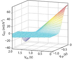
Figure 6 Third-order drain conductance of a GaAs pHEMT vs. Vds and Vgs.
Modeling the drain conductance in terms of applied gate and drain voltages can be done with a Taylor series expansion as shown below, to observe how the second- and third-order drain conductances vary.
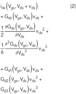
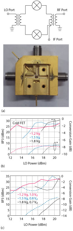
Figure 7 MMIC schematic and prototype (a), IIP3 and conversion gain vs. LO power with the drains DC grounded (b) and with drain bias applied (pinch-off = –1.2 V) (c).
The goal is to minimize third-order distortion products since they are close to the IF, thus we want to reduce the third-order drain conductance term (Gd3) as much as possible over the gate swing. Using a 4 × 25 µm FET from Qorvo’s 0.15 µm PHEMT process, the measured third-order drain conductance (Gd3) over both the applied gate and drain bias is shown in Figure 6. There is a sweet spot for these devices to achieve the lowest Gd3. Thus, with a little drain bias applied, this sweet spot should yield the lowest possible intermodulation levels achievable within the FET.
MMIC DESIGN
To demonstrate Gd3 minimization, a MMIC mixer is designed and fabricated (see Figure 7a). A single balanced resistive FET mixer topology with balanced LO and RF is chosen for its small size and ability to fit on a chip. This configuration does not provide for rejection of even-order intermodulation products, but it does improve the inherent LO-IF and RF-IF port isolations. The MMIC is fabricated using Qorvo’s 0.15 µm GaAs PHEMT process. The mixer core uses a pair of 4 × 25 µm FETs. The gates are biased through N+ doped GaAs resistors, and the drains are biased through an off-chip bias-T.
The LO and RF baluns utilize a spiral Marchand structure with capacitive compensation to improve amplitude and phase balance. This type of balun allows the mixer to work well over a multi-octave bandwidth, but requires that all the matching networks between the baluns and the FETs operate over a similar bandwidth as well. This type of balun does not inherently provide an optimal termination to the leakage that passes through Cgd, but it is an acceptable design tradeoff in terms of operating bandwidth. The RF balun is designed to allow the IF to pass through unaffected.
MMIC MEASUREMENT RESULTS
The MMIC is packaged in a fixture with 2.92 mm K connectors. Testing is done with a two-tone signal at ‐5 dBm per tone, separated by 10 MHz centered around 27 GHz. The LO is fixed at 28 GHz and is swept in power to ensure the mixer is driven sufficiently at selected gate bias points.
Figure 7b shows the measured conversion gain and IIP3 with the drains grounded (cold FET), while Figure 7c shows them with drain bias applied. In the cold FET case, as the devices are biased further below pinch-off and the LO drive level is increased both the IIP3 and conversion gain steadily improve. With drain bias applied, the conversion gain increases slightly, but the large improvement in IIP3 is a good tradeoff.
Large signal testing is conducted as well; Figure 8 shows the measured conversion gain of each mixer as a single tone 27 GHz RF signal is swept in power from 0 to 21 dBm, with a fixed 28 GHz LO. In cold FET operation, the mixer achieves an input 1 dB compression point (P1dB) of 16.5 dBm, only 0.4 dB below the LO drive level. This is one of the merits of using FETs; the RF and LO are applied to different parts of the mixer, whereas in a diode mixer both the LO and RF directly control the diode conductance. With drain bias applied the mixer achieves a P1dB of 21.7 dBm, 2 dB above the LO drive. This can be attributed to the reduction of Cgd via the application of drain bias.
Conclusion
Maximizing a mixer’s IIP3 can vastly improve the dynamic range of a system and result in overall higher system performance. The design process for producing highly linear FET resistive mixers is reviewed, and a GaAs MMIC is designed and built using the linearization techniques discussed. An IIP3 of 35 dBm is achieved in a mmWave mixer.
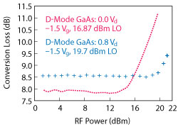
Figure 8 Measured conversion loss at 27 GHz vs. RF input power, tested in both cold FET and optimized drain bias modes.
References
- B. Henderson and E. Camargo, “Microwave Mixer Technology and Applications,” Artech House, Norwood, Mass., 2013.
- S. Peng, “A Simplified Method to Predict The Conversion Loss of FET Resistive Mixers,” IEEE MTT-S International Microwave Symposium Digest, June 1997, pp. 857–860.
- S. Maas, “A GaAs MESFET Mixer with Very Low Intermodulation,” IEEE Transactions on Microwave Theory and Techniques, Vol. 35, No. 4, April 1987, pp. 425–429.
- S. Maas, “Microwave Mixers,” Artech House, Norwood, Mass., 1993.
- S. Maas, “The RF and Microwave Circuit Design Cookbook,” Artech House, Norwood, Mass., 1998.
- J. A. Garcia, J. C. Pedro, M. L. De la Fuente, N. B. Carvalho, A. Mediavilla and A. Tazon, “Resistive FET Mixer Conversion Loss and IMD Optimization by Selective Drain Bias,” IEEE MTT-S International Microwave Symposium Digest, Vol. 2, June 1999, pp. 803–806.