
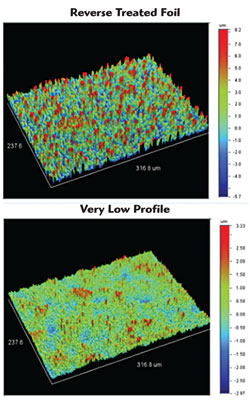
Figure 1 Comparison of the roughness of reverse treated foil (RTF) and very low profile (VLP) copper. The RTF has a root-mean-square roughness (Rrms) of 0.59 µm, with maximum height (Rz) of 3.93 µm. The VLP is better, with Rrms = 0.36 µm and Rz = 2.06 µm.
Requirements for stability of dielectric properties, manufacturability and suitability for use in hybrid technologies highlight deficiencies in current material solutions. The industry must break from its dependence on the polytetraflouroethylene (PTFE) and highly filled hydrocarbon based material solutions towards a newer set of high glass transition temperature (Tg) thermoset materials introduced to address current and future material needs.
Radio frequency printed circuit boards are typically manufactured using thermoplastic substrates such as PTFE or filled hydrocarbon based resins. These resins have excellent electrical properties but poor mechanical and thermo mechanical qualities. With the advent of new material technologies, there is a growing emphasis on the mechanical and thermal characteristics of the dielectrics as well as their electrical properties. Emerging product technologies require multilayer circuitry, hybrid RF/digital technology and increased power handling capability to be engineered into substrates.
Emerging Applications
Aerospace and defense applications have historically been the foundation for development of RF and millimeter wave technologies. In recent years, however, there has been a massive increase in commercial RF applications. With the widespread proliferation of wireless communications, commercial RF applications have grown exponentially and are moving higher in frequency. Automotive radar for example, is increasing in frequency of operation from K-Band to W-Band. V-Band ultra-broadband wireless indoor communications, microwave imaging at 94 GHz and applications at other millimeter wave frequencies are being developed as well.1 Multiple functions are integrated on single chips facilitating board integration, while exacerbating thermal management issues.
V-Band point-to-point microwave links are emerging as environmentally friendly alternatives to fiber-to-home technologies. In the U.S., U.K. and some Asian countries, the frequency band from 56 to 64 GHz is not regulated, providing opportunities for deployment of point-to-point, line of sight links with very high bandwidth and frequency reuse capability. This frequency band is known for high attenuation caused by oxygen in the atmosphere and does not allow the signal to propagate beyond a certain distance, making the communication more secure. The use of turbo coding and signal processing techniques such as the Viterbi algorithms has caused the communication bandwidths to approach the theoretical Shannon limit and the focus is now on increasing the bandwidth through smaller cells.2 These networks comprised of macro base stations coupled with micro, femto and picocells form heterogeneous networks, or HetNets. HetNets rely on very small cells which can cater to a group, office, building or a set of buildings. The communication is mainly digital and could be fed through point-to-point links or wireless links.2 The circuitry required is hybrid to a certain extent with RF or digital on the receiving or transmitting end. These heterogeneous networks are being looked at as a solution to increasing capacity and improving network coverage.
Millimeter wave frequencies present unique challenges for PCB materials. Methods and techniques are not established or standardized for measuring the dielectric properties in millimeter wave region. RF/microwave integration into ICs also affects how these materials are used.
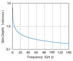
Figure 2 Skin depth as a function of frequency.
PCB Requirements
Dielectric material properties are driven by system requirements such as frequency of operation, power handling, noise, size, types of components and features. Dielectric loss, thermal stability and thermal management requirements, layer count, modulus, warp and twist requirements, and other factors go into the selection of the appropriate PCB material. Stability with humidity and temperature, power handling capability and passive intermodulation (PIM) have a bearing on material selection as well.
In addition to dielectric losses, conductor losses are becoming increasingly important. The surface roughness of copper plays a major role in increased attenuation at higher frequencies and especially in the millimeter wave region where conductor losses can dwarf dielectric losses. The skin depth at frequencies around 77 GHz is extremely small so most of the current must flow through the surface where it is strongly influenced by roughness. Figure 1 shows the surface roughness of the different types of copper used. Skin depth as a function of frequency and the effect of copper surface roughness on relative attenuation are shown in Figures 2 and 3, respectively. Figure 3 was developed using the Hammerstad and Bekkadal equation.3

where D = root mean square surface height, δs = skin depth and αc = conductor loss.
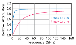
Figure 3 Relative attenuation as a function of copper surface roughness.
PIM occurs in passive devices whenever RF signals at two or more frequencies are present on a conductor. PIM is created by superimposing sine waves, creating harmonics that can add, subtract, or even cancel the desired signal. PIM causes unwanted noise, increasing the signal to noise ratio. Odd harmonics can generate spurious signals that can lead to communications interference and disruption. The use of appropriate copper with very low impurities and low roughness helps alleviate PIM.
PCBs for RF applications are typically double sided or of hybrid (multi-layer/dissimilar dielectric) construction. Hybrid PCBs, consisting of FR-4 and RF optimized substrates reduce the overall cost of materials. They are typically used for power amplifiers in cellular base stations, low noise block down converters and advanced automotive safety systems.
Chip manufacturers are packing more functionality into ICs, driving the need for PCB materials that meet both high speed digital and RF requirements. This includes predictable dimensional stability, low loss, controlled dielectric constant, lead-free construction with very tight pitches and electrochemical migration (or conductive anodic filamentation) resistance. CAF poses a major reliability risk by creating a conductive path between holes, or holes and planes.
There is an emerging need for isotropic RF substrates with higher thermal conductivity. RF boards will also see new requirements for CAF and thermal cycling reliability. PCB processes such as drilling and plating are coming under increased scrutiny to ensure reliable performance. These new requirements, coupled with the existing material challenges make RF board manufacturing increasingly more complex.
Current PCB Materials
Most dielectrics in use today are based on PTFE or highly filled hydrocarbon based resins. Another new class of products employs conventional thermoset technology to produce high glass transition polymer composites for use in these emerging applications.
PTFE/PTFE with Woven Fabrics/Filled PTFE Based Dielectrics
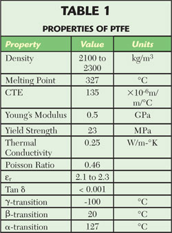
PTFE is a long chain polymer of high molecular weight. It is primarily crystalline in nature.4 It is in wide use for RF applications because of its superior electrical properties, having a low dielectric constant between 2.1 and 2.3 and a loss tangent below 0.001. These properties are stable up to millimeter wave frequencies. PTFE is traditionally used as a substrate for RF applications, including applications in space. Table 1 summarizes its properties.
Dielectric Properties: It is commonly believed that the dielectric properties of PTFE are very stable with temperature; however, there is variation. To understand this, one must look at its structure. PTFE after polymerization is almost 90 to 95 percent crystalline. Cooling down and further processing determines the degree of crystallinity at room temperature. Processing steps, such as sintering above its melting point, lead to changes in crystallinity.PTFE has a crystalline melting point at an atmospheric pressure of about 332° to 346°C for unsintered materialand about 327°C for sintered material. For 100 percent crystalline PTFE, relative densities of 2.347 at 0° and 2.302 at 25°C have been calculated from the x-ray crystallographic data. The relative density of amorphous PTFE is 2.00, as obtained by density measurements at room temperature.4 Almost all fabricated PTFE displays crystallinity within the range of 50 to 75 percent depending on the rate of cooling. The relative density of 100 percent crystalline PTFE at 23°C is 2.3 while that of 0 percent crystalline (100 percent amorphous) PTFE under the same conditions is 2.0. Therefore, the relative density of PTFE can be used to provide a simple index of crystallinity.The dielectric loss of PTFE is sufficiently low to allow the permittivity to be calculated with a high degree of accuracy using the Clausius-Mossotti formula.4,5
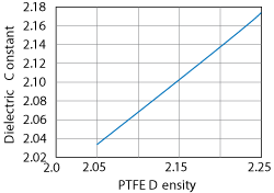
Figure 4 PTFE dielectric constant versus density.

where NA is Avogadro’s number and the quantity  is called the molar polarization (PM) and has dimensions of volume. The values for bond polarizabilities can be looked up or added up using group contributions methods.

Using this expression with a k value of 0.125,5-7 is valid only for non-polar molecules. Figure 4 shows the relationship between the density of PTFE and εr. Stability of the dielectric constant depends on the density of PTFE which changes with temperature, so the properties of PTFE are not as stable as often portrayed. The sintering process required for building the circuit boards will change the density.
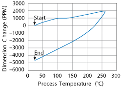
Figure 5 X-direction dimensional change versus temperature of microfiber filled PTFE.
Mechanical Properties and Creep: PTFE has a low elastic modulus of about 0.5 GPa. The coefficient of thermal expansion (CTE) is also highly variable and shows very high expansion. Until now PTFE has been the material of choice for use at millimeter wave frequencies. While PTFE may be today’s workhorse, it may not be the best choice for future applications due to issues with its mechanical and physical properties. At high temperatures, permanent deformation can occur over time at a stress level well below its yield strength. This time-dependent permanent deformation is called creep. It occurs at low stress levels and a temperature above 0.5Tm, where Tm is the absolute melting point. A polymer such as PTFE, which has a 600°K melting point, would experience creep at over 300°K or 27°C (close to room temperature). Creep is measured by loading at a constant stress level and measuring the deformation over time. Initial elastic and primary creep occur very quickly and then the creep develops at a steady state rate followed by a very steep rise leading to fracture.8 PTFE is highly prone to creep, which raises doubt concerning its suitability for demanding environments such as automotive applications that require operation in temperatures from subzero to close to 85°C. Steady state creep strain can be expressed as

where B is a constant, n is a value between 3 and 8, Qc is the activation energy in J/mol and R is the universal gas constant in J/mol/k. This equation with an exponent, n, of around 5 indicates that the creep rate can double with a modest increase of 20°C.9 The creep rate of PTFE materials makes them unsuitable for applications requiring higher temperatures as it would cause a shift in the dielectric properties.
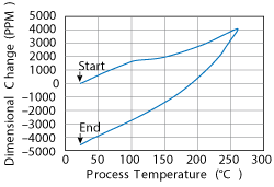
Figure 6 Y-direction dimensional change versus temperature of microfiber filled PTFE.
Processing Challenges: PTFE based materials are regarded as less desirable for multilayer PCBs due to their high cost, high CTE and processing difficulties. Therefore, the use of PTFE based laminates has been relegated to lower layer count boards. PTFE requires very high processing temperatures over 330°C and high pressure. The bonding sheets are not available and there is no flow or fill to encapsulate the traces and the circuitry. Most PTFE based laminates are available as microfiber filled sheets and therefore possess very low elastic moduli. Some laminates with dielectric constants above 3.2 use woven glass reinforcement, but this increases the dissipation factor due to the use of glass. Non-reinforced PTFE has a lower dielectric constant and dissipation factor, but due to its low modulus and very high CTE, it must be filled with ceramic fillers. Because the PTFE materials do not really bond to the filler particles and simply encapsulate them, the net effect is a reduction in PTFE polymer volume, while the overall CTE is not significantly lowered. High CTE can lead to issues such as dimensional deformation, inter-laminar shear stress when building hybrids and/or residual stresses in the board. As creep manifests itself over a longer period of time, the stress continues to relax at room temperature. This can lead to the product not performing at the optimum level over time due to creep-induced deformation. High CTE in the Z axis affects plated-through-hole reliability. Copper has a low coefficient of expansion and the mismatch leads to stresses causing fatigue failure as copper experiences high plastic strains.
Technology is shifting towards higher layer counts and sequential laminations for mixed RF/digital boards. The technology shift creates constraints on expansion; this means CTE is of special importance for these multilayer designs. Registration is of high importance as well, because of smaller pitches and pad sizes that rely on plated through-holes to create connections between the different PCB layers. PTFE laminates filled with abrasive fillers lead to high drill wear and are generally more difficult to drill. The drill bit life is substantially reduced, increasing manufacturing costs.
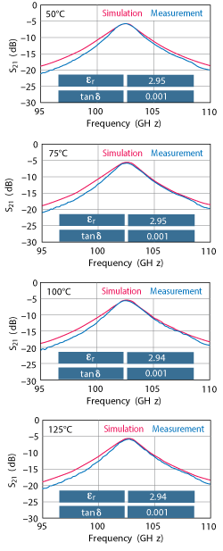
Figure 7 Simulated and measured RF properties of new thermoset material at various temperatures. Data courtesy of IZM Fraunhofer.
Dimensional Stability:The main issue with PTFE substrates is poor dimensional stability. Due to its low glass transition temperature and low yield strength, it exhibits a high degree of permanent plastic deformation. Figures 5 and 6 show deformation of a glass microfiber-filled material in the X- and Y- directions. Permanent deformation is very high, almost an order of magnitude higher than for FR-4 products. Manufacturing boards with acceptable yields is difficult and expensive. This is the single biggest challenge to using PTFE based laminates for hybrid or multilayer applications.
Highly Filled Hydrocarbon Based Resins
Hydrocarbon based resins are cross linked with other polymers to increase the Tg, but while they are are presented as high Tg materials, they have intrinsically very low Tgs. Typically, when measured using a dynamic mechanical analyzer (DMA), they will exhibit a glass transition of around 95° to 105°C. The numbers with differential scanning calorimetry (DSC) cannot be read as there is not a significant transition signal due to the amount of filler used. A thermo-mechanical analyzer (TMA) shows no inflection on the Z-axis expansion at higher temperatures but an inflection can be observed in the sub-ambient to 60°C range. This indicates a very high filler loading on a woven glass fabric with a rubbery low Tg matrix.
These laminates are used in applications such as base stations and LNBs. Since they do not have the low loss properties of PTFE or the adhesion required for the use of low profile copper, their use will be limited. Dielectric properties are not stable with temperature and have been known to shift due to oxidation under operation at modestly elevated temperatures. In fact, the laminates offered as oxidation resistant show severe discoloration upon exposure to elevated temperatures. The fillers are highly abrasive and lead to drilling issues. The drilling costs sometimes are higher than the cost of the material itself. Additional processing steps, such as plasma drilling for hole wall preparation, are expensive. The product offering does not include bonding sheets; limited offering is available for cores.
The other major issue is CTE mismatch in the building of hybrids. Because the resin matrix is highly filled, the CTE in the Z-direction is very low. Additionally, as there is no Tg above 60°C, the X and Y CTEs do not show an inflection and continue expanding at the same rate. The FR-4 type laminates undergo a transition and show a sharp increase in Z expansion and a significant drop in X and Y CTEs. When bonded together, the hybrid board experiences strain, leading to high thermal stress between the FR-4 and the ceramic filled laminates. This often results in de-lamination.
The inability to make robust hybrid boards, lack of suitable bonding sheets, higher loss, inability to use extremely low profile copper, and low dielectric stability under elevated temperature, coupled with oxidation risks will render these types of products obsolete as technology shifts to higher layer counts.
A New Class of Thermoset Polymers
Over the last few years, the market has witnessed the arrival of thermoset materials that behave like standard FR-4 materials, while delivering excellent electrical and thermo-mechanical properties. The products are thermoset systems exhibiting a Tg of around 200°C. CTEs are well controlled even for higher resin constructions. A full complement of laminates and prepregs is available including an offering for the high speed digital and RF and millimeter wave space. The products are available in a full range of dielectric constants.
Stability of Dielectric Properties Over Frequency
Dielectric properties are stable from 1 to over 100 GHz. Virtually no change is detected over the entire range. This is attributed to the fact that the products are truly high Tg thermoset polymersand therefore do not exhibit inflections in crystallinity like PTFE or the artifacts of low Tg with the highly filled hydrocarbon based resin systems. Figure 7 shows the data generated by IZM Fraunhofer Institute in the 102 to 103 GHz range. The properties are very stable and the dielectric constant and dissipation factors are virtually unchanged at high temperature.
One of the major concerns with the dielectrics is the ability to retain their properties after prolonged exposure to high temperature. Continuous operation at 85° to 125°C is a fairly common requirement. Even minor changes in dielectric properties can lead to major performance issues. As shown in Figures 8 and 9, the high Tg thermoset systems, even after prolonged exposure to high temperatures, show little or no oxidative or other degradation. Changes in dielectric properties are minimal in comparison to the PTFE or highly filled hydrocarbon based products.
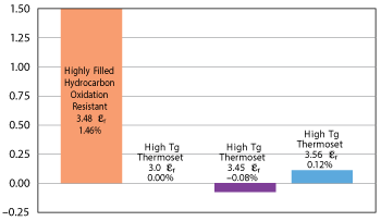
Figure 8 Change in dielectric constant for various materials, measured at 10 GHz following 1000 hours of aging at 125°C.
Insertion Loss and Power Handling
Conductor loss not only contributes to overall loss but also increases power dissipated into the board, leading to undesirable temperature increases and power handling limitations. Due to conductor surface roughness, there is also an increase in parasitic capacitance; and the phase constant (β) changes with frequency affecting phase velocity and group velocity as well.10 The solution is to use as low a profile of copper as possible. However, this is not straightforward because the resin system must bond securely with very low profile copper, without requiring any special treatment.
The newer thermoset systems are unique in the sense that they provide high peel strengths even for the smoothest copper available. These products are more advantageous for millimeter wave applications, as extremely low profile copper with Rz values below 1.5 µ can be used. These Rz values are lower than the rolled annealed copper that was once considered the benchmark. The rolled annealed copper is only available in small formats and requires special treatment for bonding.
With low profile copper, insertion loss goes down substantially. Energy from conductor and dielectric loss is dissipated in the dielectric, leading to dielectric heating.3,11,12 Reduced conductor loss, therefore, increases the power handling capability. Figure 10 compares a high Tg thermoset transmission line with one using a filled (non woven) PTFE dielectric. The power handling capability of microstrip lines can be obtained by taking Equation 11, and setting the thickness d=0.11
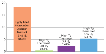
Figure 9 Change in dielectric loss for various materials, measured at 10 GHz following 1000 hours of aging at 125°C.

where K is the dielectric thermal conductivity W/m-°K, αc , αd are the conductor and dielectric losses, we is the effective width and h is the height, average power handling is given by

Figure 11 compares the power handling of a filled PTFE microstrip line with that of a high Tg thermoset low loss microstrip line. Higher power handling in the thermoset PCB is enabled by its higher thermal conductivity and use of very smooth, high peel strength copper.
Processing and Cost of Ownership
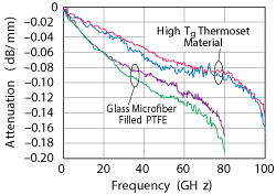
Figure 10 Attenuation versus frequency of high Tg thermoset and glass microfiber filled PTFE. Data courtesy of Freescale Semiconductor.
The ease of processing and availability of choices is a big factor in the fast adoption of these new products. Dimensional stability is very predictable, leading to high yields. Drilling costs are much lower due to the fact that the products have low filler loading. The melt viscosity is in the same range as FR-4 type systems with similar flow and fill behavior. Processing does not require the use of plasma; the standard desmear process is suitable.
Because CTEs are in the same range as standard FR-4 materials, with similar thermo-mechanical properties, the ability to make reliable hybrid boards is straightforward. Creep does not manifest itself as the Tg, at 200°C, is sufficiently high. A number of OEMs are adopting these products for automotive radars, phased array antennas, sensors, base station power amplifier boards and other RF applications. Customers are reporting significant cost savings.
Conclusion
A new enabling technology employs a thermoset matrix that has very good adhesion to metals, enabling the use of copper with extremely smooth surfaces. The industry is increasingly seeing hybrid boards combining RF and digital technology. The increasing integration of functionality into single chips is making it easier to combine the digital and RF circuitry on the same board. Conventional RF substrates such as PTFE are not suitable for hybrid technology, as the layer count is high and bonding sheets are not available. Also, the manufacturing costs of boards made using PTFE or the hydrocarbon based resin alternatives are high. Yields are poor due to the dimensional stability issues, and the systems tend to be unreliable.
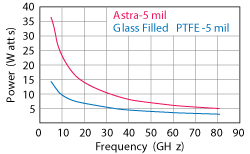
Figure 11 Maximum power handling of 5 mil, 50 ohm microstrip lines at 85°C for glass filled PTFE and Astra MT300.
There is a strong need for non-PTFE and non-thermoplastic based substrates with dielectric properties similar to PTFE. Thermoset systems, which display high glass transition temperatures and high thermal reliability, while maintaining stability in dielectric properties over a higher range of temperatures and frequencies, are quickly being adopted.
Acknowledgment
The author would like to acknowledge the help and support from the Analytical Services Lab at Isola USA Corp. in providing data and helping to carry out experiments.
References
- G. Kouemou, “Radar Technology,” InTech, Chapter 15, Jan 2010. Available at: www.intechopen.com/books/radar-technology/planar-antenna-technology-for-mm-wave-automotive-radar-sensing-and-communications.
- R. Q. Hu and Y. Qian, “Heterogeneous Cellular Networks,”John Wiley and Sons, 2013.
- T. C. Edwards and M. B. Steer, “Foundations of Interconnect and Microstrip Design,”Third Edition, John Wiley and Sons, 2000.
- “Physical Properties of Fluon Unfilled and Filled PTFE,” Processing Note, www.agcchem.com/newsroom/finish/13-fluon-ptfe-resins/46-processing-note-f12-135.
- L. H. Sperling, “Physical Polymer Science,”Fourth Edition, John Wiley and Sons, 2006.
- D.W. van Krevelen, “Properties of Polymers,”Elsevier B.V., Amsterdam, 2000.
- C. K. Kwan, “Dielectric Phenomena in Solids,”Elsevier Academic Press, London, 2004.
- T. Blythe and D. Bloor, “Electrical Properties of Polymers,”Cambridge University Press, 2005.
- M. Ashby, H. Shercliff and D. Cebon, “Materials Engineering, Science, Processing and Design,”Butterworth-Heinemann, 2007.
- J.M. Jin, Jiang-Meng, “Theory and Computation of Electromagnetic Fields,”John Wiley and Sons, 2010.
- I. J. Bahl, “Average Power Handling Capability of Multilayer Microstrip Lines,” International Journal of RF and Microwave Computer-Aided Engineering, Vol. 11, No. 6, November 2001, pp. 385–395.
- D. M. Pozar, “Microwave Engineering,”Fourth Edition, John Wiley and Sons, 2010.