
InP-based HBT Technology for Next-generation Lightwave Communications
InAlAs/InGaAs-InP heterojunction bipolar transistor (HBT) technology offers high device speed, low 1/f flicker noise and monolithic integration of 1.55 mm InGaAs photodetectors making them well suited for next-generation, high data rate optoelectronic communication links. Application toward next-generation > 40 Gbps communication systems is discussed, and state-of-the-art receiver capability is presented.
K.W. Kobayashi, A.K. Oki, A. Gutierrez-Aitken, J. Cowles, L.T. Tran, T.R. Block and D.C. Streit
TRW Electronics Systems & Technology Division
Redondo Beach, CA
Today’s state-of-the-art performance in optoelectronic communications concentrates on 40 Gbps optoelectronic data links and greater using III-V semiconductor technologies, including GaAs- and InP-based MESFET, high electron mobility transistor (HEMT) and HBT technologies. InP-based technologies are attractive because they have the potential to integrate narrow band gap
InGaAs photodiodes, which are compatible with the detection of 1.30 to 1.55 m m long-wavelength light. In addition, the inherent properties of InP (which possesses higher electron velocities, narrower band gaps and lower surface recombination velocities than GaAs) make InP-based technologies attractive for high speed and low DC power digital and analog electronics.
InP-based HBTs typically have a vertical molecular beam epitaxy (MBE) device profile and exhibit low surface recombination and low 1/f flicker noise. These devices can produce digital and analog signal processing circuits that exhibit the low phase jitter and high receiver sensitivity characteristics of conventional silicon bipolar technologies but with greater speeds. These fundamental properties make InP HBT technology attractive for next-generation high speed digital communications. This article describes recent advances in InAlAs/InGaAs-InP HBT technology, revealing the performance capability of key optoelectronic HBT MMICs critical for next-generation, high speed lightwave communications.
InP-based HBT IC Technology
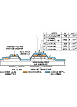 The MMICs reported in this article are based on InAlAs/InGaAs-InP HBT device technology. Figure 1 shows a cross section of TRW’s InAlAs/InGaAs HBT device structure. This vertical epitaxy structure is compatible with the monolithic integration of high performance InGaAs PIN photodetectors without requiring additional epitaxy regrowth. The InAlAs/InGaAs HBT device epitaxy structure is grown using MBE on a semi-insulating, three-inch InP substrate. Be and Si are used as p- and n-type dopants for the base and emitter/collector, respectively.
The emitter incorporates a 750 Å InGaAs cap, which is highly doped to obtain low emitter contact resistance. The intrinsic emitter region is 1900 Å thick and doped to 5 x 1017 cm–3 . The base-emitter junction is graded compositionally from InGaAs to InAlAs to form HBTs with repeatable beta and low Vbe characteristics. The base-collector epitaxial structure comprises a base thickness of 800 Å uniformly doped to 3 x 1019 cm–3 , a 7000 Å-thick n-type collector lightly doped to 1 x 1016 cm–3 and an n+ subcollector doped to 5 x 1018 cm–3 . The HBT DC beta across the wafers is typically > 25 at a current density of Jc = 40 kA/cm2 . The breakdown voltage BVceo is approximately 8 V and the BVcbo is approximately 13 V, which is more than adequate for most analog applications.
A fully self-aligned HBT process is used to produce 1 m m emitter-width HBTs, which feature an HBT base-mesa undercut profile that enables a 30 to 40 percent reduction in Ccb capacitance and produces improved device fT and fmax as well as better circuit performance.1 The 1 m m emitter-width base-undercut HBTs have obtained peak fT s and fmaxs of 80 and 200 GHz (from unilateral gain), respectively. These numbers were achieved from a 1 x 10 m m2 quad-emitter HBT biased at a current density of Jc that is  approximately equal to 50 to 60 kA/cm2 and a Vce equal to 2.0 V.
Figure 2 shows a comparison of device fT and fmax capability for both AlGaAs/GaAs and InAlAs/InGaAs-InP HBTs. Appreciable performance can be obtained by scaling the device emitter width as illustrated by the 2 and 1 m m emitter-width GaAs HBT cases. However, a more dramatic performance improvement is observed when employing the higher electron velocity InP-based HBT structure. The higher  electron velocities of InP-based HBTs enable them to achieve device and circuit speeds required for ³ 40 Gbps communication data rates while relying on relaxed and highly reproducible 1 m m emitter-width process lithography.
Optoelectronic Receiver and Transmitter Architecture and Technology Partition
Figure 3 shows a block diagram of an optoelectronic communication link, which includes a modulator transmitter and a photodetector receiver with clock and data recovery. While GaAs HBT and HEMT technologies have been able to produce many of these IC components with operation up to 40 Gbps,2–4 InAlAs/InGaAs-InP HBTs offer the potential for higher circuit speeds with lower DC power and a higher complexity single-chip receiver solution including clock and data recovery functions as shown.
|
Table I | ||||
|
Device Properties |
GaAs |
InP |
InP |
Circuit Performance Leverage |
|
FT /fmax |
Medium |
High |
Very High |
High speed/bandwidth - all circuits |
|
Threshold matching and uniformity |
Excellent |
Excellent |
Poor |
Signal/noise, BER, sensitivity (signal ambiguity) of clock/data recovery |
|
Low noise figure |
Fair |
Fair |
Excellent |
Low noise pre-amplifier (meaningful in low impedence system) |
|
Low I/f noise |
Good |
Good |
Poor |
High signal/noise, low BER in transimpedance/pre-amplifier |
|
Vertical PIN diode |
Yes |
Yes |
No |
High responsitivity, monolithic compatibility- low cost |
|
Breakdown voltage |
High |
Low |
Low |
5 V p-p driving voltage required for modulator and laser drivers |
|
Low DC power |
Fair |
Good |
Good |
High speed/low DC power |
Table 1 lists a comparison of the inherent device properties of GaAs HBTs, InP HBTs and InP HEMTs in relation to the pertinent optoelectronic circuit applications. While HEMTs offer the higher frequency operation and lower noise figures required for low noise mm-wave applications, InP HBTs offer better analog characteristics such as the threshold matching necessary for high input sensitivity analog performance while also providing the low phase noise characteristic of the HBT device. Moreover, the inherent MBE-based structure of HBTs is compatible monolithically with the fabrication of high responsivity vertical PIN diode photodetectors. Wide band gap GaAs HBTs can accommodate monolithic photodetection in the 0.9 mm wavelength range while InGaAs/InP HBTs can accommodate longer 1.3 to 1.55 m m lightwave detection, which is often more desirable due to its lower attenuation in single-mode fiber applications. However, a more practical reason for using 1.55 m m wavelength systems is that erbium-doped fiber-optic amplifiers are more readily available for both high power and low noise applications. This availability is attractive for both laser and fiber-optic communications.
On the other hand, GaAs HBTs, while not as fast, possess higher breakdown voltage characteristics, which are attractive for laser drivers in direct modulation and electro-optic modulator drivers in indirect modulation transmitter applications. Thus, GaAs HBTs are well suited for transmitter applications while InP-based HBTs are well suited for the low cost, single-chip receiver solution for high data rate  lightwave communication systems.
Fundamental InP HBT Characteristics
One of the key advantages of InP- vs. GaAs-based HBTs is the InP-based HBTs’ high frequency performance under very low DC power operation. Low DC power is important particularly in space and satellite applications. Figure 4 shows the lower bipolar turn-on voltage of InGaAs/InP HBTs (which can obtain turn-on voltages as low as 0.4 to 0.6 V) while their AlGaAs/GaAs HBT counterpart has approximately twice the  turn-on voltage in the 1.1 to 1.3 V range. The low Vbe of InGaAs-InP HBTs combined with their high electron velocity allow high frequency device performance under very low DC voltage operation near the transistor’s saturation voltage Vce (sat). Figure 5 shows that device fT s of greater than 30 GHz can be maintained at a low Vce operating voltage of 0.5 V and at a low current density of 25 kA/cm2 .
A direct consequence of these characteristics is that InP-based HBTs can achieve a very high amplifier gain-bandwidth product per DC power ratio (GBP/Pdc ) for low supply voltage operation under 3 V. This characteristic is shown in Figure 6 , which compares InP HBT direct-coupled amplifiers5 with other technologies,2,6–11 including GaAs- and SiGe-based bipolar junction transistors (BJT) and HBTs. Similar low DC power performance benefits are expected for higher complexity InP HBT digital and analog circuits as well.
A key characteristic that makes InP HBTs attractive for clock and data recovery applications is their low noise 1/f noise corner frequencies and low 1/f flicker noise. The 1/f noise corner frequency of GaAs and InP HBTs typically is several orders of magnitude better than MESFET and HEMT devices. This characteristic is shown in Figure 7 , which gives the typical broadband device noise characteristics of InP HBTs compared to 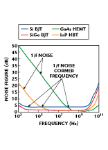 conventional Si and SiGe BJTs and HEMT devices. The noise corner frequency denotes approximately the lowest frequency at which a circuit may operate without incurring substantial noise degradation.
A low transistor 1/f flicker noise corner frequency is attractive for digital communications, which require broadband performance from DC to approximately 70 percent of the highest bit rate. The 1/f flicker noise characteristics are desirable for achieving low phase noise in oscillators as well as low phase jitter in clock and data recovery-type circuits. Both can determine the overall bit error rate (BER) of the system even when the technology provides ample bandwidth. Although the low frequency noise of HBTs is not nearly as good as the best conventional silicon bipolar devices, HBTs obtain much higher cutoff frequencies, which enable the higher data rate applications.
Another key HBT device property that impacts the resolution, accuracy and precision with which clock, data and retiming circuits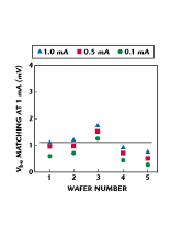 operate is the inherently uniform bipolar device threshold characteristics. The device threshold voltage of HBT and conventional bipolar devices are determined by the band gap characteristics of the base material and, therefore, are less process sensitive than FET devices. Threshold voltages of GaAs and InP HBTs typically have 1-sigma variations of approximately 1 mV from wafer to wafer. Figure 8 shows the wafer-to-wafer threshold uniformity of InP HBTs that typically have a 1-sigma variation less than 1.5 mV. This threshold uniformity is at least an order of magnitude better than typical MESFET or HEMT device threshold variations. The threshold uniformity matching is critical in determining the signal ambiguity level of comparators in analog-to-digital converters as well as clock and data recovery circuits that employ threshold decision functions. The sensitivity of these circuits becomes a function of frequency and input power. Having better threshold uniformity or higher sensitivity allows higher speeds without requiring large input voltage swings to compensate for degraded input insensitivity.
In most device technologies, a trade-off between device speed fT and breakdown voltage usually exists. HBT device technologies possess the freedom to redesign the device for higher speed by optimizing the epitaxy structure. This optimization often comes at the expense of the device’s breakdown voltage. While high speed circuit performance has been demonstrated from frequency-optimized silicon-based technologies, these technologies often will fall short of providing adequate voltage swing, which is limited by the practical breakdown characteristics of the device. An example is the use of SiGe-based HBT technology to enhance fT but at the expense of  breakdown voltage. The inadequate voltage swing can preempt these technologies from applications requiring moderate voltage swings, especially at high frequencies where signal ambiguity (sensitivity) becomes an issue.
Figure 9 shows the device fT vs. breakdown voltage for various bipolar device technologies. Typical GaAs- and InP-based HBTs show a factor of 2 better fT -breakdown product at higher frequencies than conventional silicon and SiGe bipolar technologies. At 100 GHz fTs, the InP HBTs demonstrate breakdowns of approximately 7 V while SiGe BJTs demonstrate only 2 to 3 V breakdowns. Because of the flexibility of MBE, InP HBTs employing a double-HBT (DHBT) structure can significantly enhance the fT -breakdown product with fT s of 140 and 220 GHz, with corresponding breakdown voltages of > 5 and > 8 V, respectively.12,13 Therefore, InP HBTs can provide the best combination of speed and breakdown, which is attractive for high speed modulator and laser driver applications.
Key InP HBT optoelectronic Performance
The maximum data rates allowed by a given device technology for optoelectronic lightwave applications typically are limited by the circuit speed of the clock and data recovery ICs, while the key IC components that determine the dynamic range of the optoelectronic receiver are the photodetector and/or preamplifier. However, while achieving high bandwidth and optimum sensitivity in the design of a photoreceiver are basic goals, other considerations influence the details of the design and, in fact, may produce a practical receiver with less than optimum performance. Examples of such considerations include dynamic range, fabrication complexity, packaging, size and weight. The monolithic integration of a photodetector and a preamplifier minimizes some of these restrictions and has many advantages over hybrid circuits such as reduction of parasitic elements and cost and increased reliability and production yield, which are particularly important in photoreceiver arrays.
An attractive feature of InP HBTs is that they are based on a vertical MBE structure as opposed to a planar FET or HEMT structure and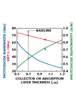 are compatible with the monolithic integration of high performance PIN diode photodetectors. A low cost, single-chip photoreceiver solution including clock and data recovery functions can be realized without the use of fancy and costly selective MBE-metal-organic chemical vapor deposition regrowth techniques.24
For the InGaAs PIN-compatible InP HBT technology, an inherent trade-off exists between the diode photoresponsivity and the bandwidth capability of the HBT and PIN diode devices that is dependent on the InGaAs collector i-region thickness. Figure 10 shows the typical trade-off between HBT and PIN cutoff frequency performance and the InGaAs PIN photodetector responsivity. For an InGaAs i-region baseline 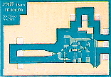 thickness of 0.7 mm, the TRW HBTs achieve an fT of 70 GHz while the InGaAs PIN diode photodetector achieves a transit-time limited bandwidth of 45 GHz and a responsivity of 0.57 A/W. This performance is more than adequate to support greater than 40 Gbps optoelectronic communication systems. Figure 11 shows an example of a monolithic integrated
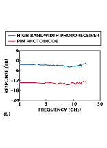 PIN diode/transimpedance amplifier photoreceiver that obtains an effective transimpedance of 44 dB-W and a 3 dB bandwidth > 20 GHz. This design uses a conventional lumped-element analog amplifier circuit topology, which is popular at 10 Gbps data rates and below.
As the speed of the device technology extends into the mm-wave region where the wavelength of the highest bit rate is on the order of the dimensions of the IC, circuit performance becomes limited due to interconnect parasitics that interact with the intrinsic device capacitive parasitics. This limitation creates premature roll-off in circuit performance well below the device’s cutoff frequency. Compounding the problem is the complex multipole/zero characteristics of these multitransistor analog topologies. A shift in the design paradigm from relying solely on conventional analog IC topologies to the use of microwave techniques is required to fully exploit the analog-to-digital speed performance offered by the advanced III-V device technologies. In particular, the use of a microwave distributed transmission line approach such as that found in distributed traveling-wave amplifiers enables the designer to fully exploit the device performance without incurring degradation due to interconnect and device parasitic effects.14
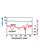 Figure 12 shows the response of an InP HBT-based distributed amplifier (DA), which achieves a gain of 6 to 7 dB and a bandwidth > 50 GHz. The corresponding transimpedance is 38 dB-W . The InP HBT DA design approach that absorbs the interconnect and device parasitics into the design achieves the widest transimpedance bandwidth and is nearly twice the bandwidth of conventional analog topologies using the same technology. Moreover, the InP-based HBT DA approach obtains a bandwidth slightly better than that obtained
 using HEMT device technology,21 which possesses much higher fTs and relies on more performance-sensitive 0.1 to 0.2 mm electron beam lithography process technology. Figure 13 shows the transimpedance amplifier bandwidth performance based on state-of-the-art device technologies.1,5,15–21
Figure 14 shows the state-of-the-art monolithically integrated PIN photoreceivers to date.22–25 A record monolithic photoreceiver bandwidth of 27 GHz has been achieved using InAlAs/InGaAs heterostructure FETs (HFET) and a distributed traveling-wave amplifier  approach.24
For comparison, the simulation capability of a monolithic photoreceiver25 based on an InP HBT distributed preamplifier and an integrated InGaAs PIN photodetector is also included. The detailed simulation of this monolithic photoreceiver is shown in Figure 15 and suggests a photoreceiver bandwidth capability of 47 GHz. This capability improves the state of the art by 74 percent and can accommodate next-generation lightwave communication systems operating at data rates up to 65 Gbps. Figure 16 shows the corresponding microphotograph of the fabricated 47 GHz photoreceiver, which employs the distributed preamplifier approach. Measurement capability at these speeds is difficult to achieve, but on-wafer optoelectronic measurement verification is planned. Future higher complexity receiver architectures with integrated clock and data recovery to accommodate the 47 GHz detector/preamplifier capability are also under development.
Conclusion
InP-based HBTs possess key device properties that are attractive for next-generation, > 40 Gbps optoelectronic communication systems. A shift in design paradigm from conventional analog topologies to a combination of analog and RF microwave approaches is required to fully exploit the speed performance offered by advanced III-V-based semiconductors such as InP HBTs. Because of the compatibility of InP HBTs with InGaAs photodetectors, a high performance, low cost monolithic photoreceiver chip solution can be realized that includes the clock and data recovery functions. Photoreceiver capability up to 47 GHz was presented based on existing InAlAs/InGaAs-InP HBT technology, which accommodates data rates in excess of 60 Gbps.
Acknowledgment
The authors wish to thank T. Naeole for InP HBT wafer processing, N. Nguyen for backside processing and C. Sieg for layout support.
References
1. K.W. Kobayashi, J. Cowles, L.T. Tran, T.R. Block, A.K. Oki and D.C. Streit, "A 2 to 50 GHz InAlAs/InGaAs-InP HBT Distributed Amplifier," 1996 IEEE GaAs IC Symposium Digest, Orlando, FL, pp. 207–210.
2. Y. Matsuoka and E. Sano, "High Speed AlGaAs/GaAs HBTs and Their Applications to 40 Gbit/s-class ICs," 1994 IEEE GaAs IC Symposium Digest, Philadelphia, PA, pp. 186–189.
3. T. Otsuji, E. Sano, Y. Imai and T. Enoki, "40 Gbit/s ICs for Future Lightwave Communications Systems," 1996 IEEE GaAs IC Symposium Digest, Philadelphia, PA, pp. 186–189.
4. T. Swahn, T. Lewin, M. Mokhtari, H. Tenhunen, R. Walden and W. Stanchina, "40 Gb/s, 3 V InP HBT ICs for a Fiber-optic Demonstrator System," 1996 IEEE GaAs IC Symposium Digest, Orlando, FL,
pp. 125–128.
5. K.W. Kobayashi, L.T. Tran, J. Cowles, T.R. Block, A.K. Oki and D.C. Streit, "Low DC Power High Gain Bandwidth Product InAlAs/InGaAs-InP HBT Direct-coupled Amplifiers," 1996 IEEE GaAs IC Symposium Digest, Orlando, FL, pp. 141–144.
6. M. Rodwell, J.F. Jensen, W.E. Stanchina, R.A. Metzger, D.B. Rensch, M.W. Pierce, T.V. Kargodorian and Y.K. Allen, "33 GHz Monolithic Cascode AlInAs/GaInAs Heterojunction Bipolar Transistor Feedback Amplifier," IEEE BCTM Digest, Minneapolis, MN, 1990, pp. 252–255.
7. R.K. Montgomery, D.A. Humphrey, P.R. Smith, B. Jalali, R.N. Nottenburg, R.A. Hamm and M.P. Panish, "A DC to 20 GHz High Gain Monolithic InP/InGaAs HBT Feedback Amplifier," IEEE IEDM Digest, pp. 36.5.1–36.5.4.
8. N.H. Sheng, W.J. Ho, N.L. Wang, R.L. Pierson, P.M. Asbeck and W.L. Edwards, "A 30 GHz Bandwidth AlGaAs/GaAs HBT Direct-coupled Feedback Amplifier," IEEE MGW Letters, Vol. 1, No. 8, August 1991, pp. 208–210.
9. Y. Kuriyama, J. Akagi, T. Sugiyama, S. Hongo, K. Tsuda, N. Iizuka and M. Obara, "DC to 40 GHz Broadband Amplifiers Using AlGaAs/GaAs HBTs," 1994 IEEE GaAs IC Symposium Digest, Philadelphia, PA, pp. 299–302.
10. H. Schumacher, A. Gruhle, U. Erben, H. Kibbel and U. Konig, "A 3 V Supply Voltage, DC to 18 GHz Si-Ge HBT Wideband Amplifier," 1995 IEEE BCTM Digest, Minneapolis, MN, pp. 190–193.
11. J.R. Long, M.A. Copeland, S.J. Kovacic, D.S. Malhi and D.L. Harame, "RF Analog and Digital Circuits in SiGe Technology," 1995 IEEE ISSC Conference, San Jose, CA, pp. 82–83.
12. S. Yamahata, K. Kurishima, H. Nakajima, T. Kobayashi and Y. Matsuoka, "Ultra-high fmax and fT InP/InGaAs Double-heterojunction Bipolar Transistors with Step-graded InGaAsP Collector," 1994 IEEE GaAs IC Symposium Digest, Philadelphia, PA, pp. 345–348.
13. S. Yamahata, K. Kurishima, H. Ito and Y. Matsuoka, "Over 220 GHz fT and fmax InP/InGaAs Double-heterojunction Bipolar Transistors with a New Hexagonal-shaped Emitter," 1995 IEEE GaAs IC Symposium Digest, San Diego, CA, pp. 163–166.
14. C.S. Aitchinson, "Potential of the Distributed Amplifier as a Photo Diode Detector Amplifier in High Bit Rate Optical Communication Systems," Electronics Letters, Vol. 26, No. 2, September 1990, pp. 1693–1695.
15. R.K. Montgomery, A. Feygenson, P.R. Smith, R.D. Yadvish, R.A. Hamm and H. Temkin, "A 28 GHz Transimpedance Preamplifier with Inductive Bandwidth Enhancement," IEEE IEDM, 1992, pp. 16.1.1–16.1.4.
16. M. Soda, H. Tezuka, F. Sato, T. Hashimoto, S. Nakamura, T. Tatsumi, T. Suzaki and T. Tashiro, "Si-analog ICs for 20 Gbps Optical Receiver," IEEE JSSC, Vol. 29, No. 12, December 1994, pp. 1577–1582.
17. A.L. Gutierrez-Aitken, K. Yang, X. Zhang, G.I. Haddad, P. Bhattacharya and L.M. Lunardi, "16 GHz Bandwidth InAlAs-InGaAs Monolithically Integrated PIN/HBT Photoreceiver," IEEE Photonics Technical Letters, Vol. 7, No. 11, November 1995, pp. 1339–1341.
18. Y. Suzuki, H. Shimawaki, Y. Amamiya, K. Fukuchi, N. Nagano, H. Yano and K. Honjo, "An HBT Preamplifier for 40 Gbps Optical Transmission Systems," 1996 IEEE GaAs IC Symposium Digest, Orlando, FL, pp. 203–205.
19. K.W. Kobayashi, L.T. Tran, M.D. Lammert, A.K. Oki and D.C. Streit, "Transimpedance Bandwidth Performance of an HBT Loss-compensated Coplanar Waveguide Distributed Amplifier," 1996 IEE Electronics Letters, Vol. 32, No. 24, November 21, 1996.
20. Z. Lao, M. Berroth, V. Hurm, A. Thiede, R. Bosch, P. Hofmann, A. Hulsmann, C. Moglestue and K. Kohler, "25 Gbps AGC Amplifier, 22 GHz Transimpedance Amplifier and 27.7 GHz Limiting Amplifier ICs Using AlGaAs/GaAs HEMTs," 1997 IEEE ISSCC Digest, San Francisco, CA, pp. 356–357.
21. S. Kimura, Y. Imai, Y. Umeda and T. Enoki, "A DC to 50 GHz InAlAs/InGaAs HEMT Distributed Baseband Amplifier Using a New Loss Compensation Technique," 1996 IEEE GaAs IC Symposium Digest, Orlando, FL, pp. 96–99.
22. A.L. Gutierrez-Aitken et al., "Wide Bandwidth InAlAs/InGaAs Monolithic PIN-HBT Photoreceiver," Proceedings of IEEE/LEOS Summer Topical Meetings: ICs for New Age Lightwave Communications, Keystone, CO, August 1995.
23. E. Sano, M. Yoneyama, S. Yamahata and Y. Matsuoka, "23 GHz Bandwidth Monolithic Photoreceiver Compatible with InP/GaAs Double Heterojunction Bipolar Transistor Fabrication Process," Electronics Letters, Vol. 30, No. 24, November 1994, pp. 2064–2065.
24. S. van Waasen, A. Umbach, U. Auer, H.G. Bach, R.M. Bertenburg, G. Janssen, G.G. Mekonnen, W. Passenberg, R. Reuter, W. Schlaak, C. Schramm, G. Unterborsch, P. Wolfram and F.J. Tegude, "27 GHz Bandwidth High Speed Monolithic Integrated Optoelectronic Photoreceiver Consisting of a Waveguide Fed Photodiode and an InAlAs/InGaAs-HFET-traveling-wave Amplifier," 1996 IEEE GaAs IC Symposium Digest, Orlando, FL, pp. 258–261.
25. K.W. Kobayashi, J. Cowles, L.T. Tran, A. Gutierrez-Aitken, T.R. Block, A.K. Oki and D.C. Streit, "A 50 MHz to 55 GHz Multi-decade InP-based HBT Distributed Amplifier," IEEE MGW Letters, 1997.
Kevin W. Kobayashi received his BSEE degree from the University of California at San Diego and his MSEE degree from the University of Southern California in 1986 and 1991, respectively. Since 1986, he has been working at TRW on the design and insertion of HBT, HEMT and MESFET MMICs into the company’s systems. Currently, Kobayashi is a senior technical specialist focused on the development of HBT MMIC design and device technology.
Aaron K. Oki received his BS from the University of Hawaii, Manoa and his MS in electrical engineering and computer science from the University of California, Berkeley in 1983 and 1985, respectively. Since joining TRW as a member of the technical staff in 1985, he has been working on production and advanced development of HBT technology. Currently, Oki is assistant manager of TRW’s microelectronic products and technology development department.
Augusto Gutierrez-Aitken received his BSEE with highest honors and his licentiature degree in electronic systems engineering from EMI University, La Paz, Bolivia, in 1985 and 1987, respectively. He also received his MSEE and PhD degrees from the University of Michigan, Ann Arbor in 1991 and 1994, respectively. Gutierrez-Aitken was a postdoctoral research fellow at the Solid State Electronics Laboratory at the University of Michigan from 1994 to 1996 where he worked on high speed and low crosstalk PIN/HBT photoreceiver arrays and high speed InP-based lasers. In 1996, he joined TRW Space and Electronics Group to work on high performance HBTs and photodiodes in compound semiconductors.
John C. Cowles graduated summa cum laude with a BS degree in electrical engineering from the University of Pennsylvania, Philadelphia in 1987. He received his MS and PhD degrees in electrical engineering from the University of Michigan, Ann Arbor in 1989 and 1994, respectively. In 1994, Cowles joined the TRW RF Product Center where he is currently working on the fabrication and characterization of advanced GaAs and InP HBT technologies for MMICs and analog and high speed digital circuits.
Liem T. Tran received his BS degree in applied physics from the California Institute of Technology and his MS degree in electrical engineering from the University of California, Berkeley. He has been with TRW since 1988 working on GaAs and InP-based HBT advanced technology development. Currently, Tran is section manager of the company’s R&D advanced III-V fabrication processes.
Thomas Ray Block received his BSEE, MSEE and PhD degrees from the University of Texas at Austin in 1984, 1986 and 1991, respectively. In 1991, he joined TRW as a senior member of the technical staff engaged in molecular beam epitaxy growth of compound semiconductors for both research and production. In 1995, Block became manager of the company’s advanced materials section.
Dwight C. Streit received his PhD degree in electrical engineering from the University of California, Los Angeles in 1986. Currently, he is manager of the microelectronics product and technology development department in TRW’s RF Products Center where he is principal investigator for several research and development projects related to III-V materials, monolithic HEMT-HBT integrated circuits and quantum effect devices.