
A new double balanced mixer (DBM) operating from 3.1 to 10.6 GHz utilizes a compact planar balun. To meet the requirements for ultra-wideband operation and improve return loss, a T-junction formed by side coupled slotlines (SCSL) and microstrip with a wideband microstrip to SCSL transition is employed. The balun’s balanced ports are in the form of adjacent microstrip lines located on the same side as the double balanced mixer. This is a practical advantage because it eliminates the crossing of the transmission lines making it more suitable for MIC design. The mixer exhibits a conversion loss of less than 13 dB from DC to 100 MHz IF. Port-to-port isolation is better than 25 dB over the RF and LO bandwidths of 3.1 to 10.6 GHz.
Ultrawideband (UWB) radio technology is becoming more popular for high speed wireless connectivity since the Federal Communications Commission approved the unlicensed operating band from 3.1 to 10.6 GHz in February 2002.1 The mixer, which provides down-conversion for the receiver and up-conversion for the transmitter, is an important component of a UWB communication system. The double balanced mixer (DBM) is the most attractive choice because of its superior suppression of spurious mixing products, wider dynamic range, excellent local oscillator (LO) noise rejection and good port-to-port isolation.2 Moreover, the double balanced configuration allows overlapping of radio frequency (RF) and LO frequency bands for efficient expansion of operational bandwidth.
Essential to the operation of a double balanced mixer, the balun converts an unbalanced signal to a balanced one and vice versa. Various types of baluns for wideband performance have been reported over the past decade. Maas2 introduced a double balanced ring mixer using a nonplanar microstrip to parallel-strip balanced transmission line balun, but it is not convenient for connection with other devices and integration with other circuits. Kim et al.3 described a planar balun based on a microstrip-to-coplanar stripline (CPS) transition, but it does not prevent the IF from being short-circuited to ground through the microstrip line, it occupies a large circuit area, and it is not suitable for MIC design. Bialkowski and Ogawa4 reported on an out-of-phase Wilkinson power divider constructed with wideband microstrip-to-slotline transitions, however, the use of only one slotline introduces more insertion loss and has poor return loss, while the balanced ports being on opposite sides makes the connection of diodes inconvenient. By effectively using coupled slot lines, Aikawa and Ogawa5 introduced a new MIC magic-T, which is useful for the design of the balun.
This article describes a compact planar balun with the balanced ports located on the same side and having a return loss much lower than that reported by Kim et al.3 A T-junction formed by side coupled slot lines (SCSL) and microstrip accompanied by a wideband microstrip to SCSL transition6,7 is used to construct a compact UWB planar balun with reduced insertion loss. It can easily be made to operate up to millimeter wave frequencies utilizing photolithographic techniques. A DBM based on this balun achieves LO/RF, LO/IF and RF/IF isolation of greater than 25 dB and conversion loss of less than 13 dB over an RF and LO frequency range of 3.1 to 10.6 GHz and an IF band of DC to 100 MHz. The proposed technique has a more convenient circuit layout and provides better performance than a conventional DBM.
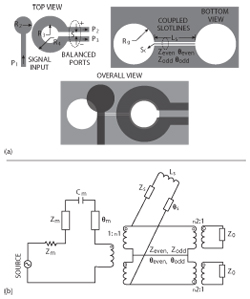
Figure 1 UWB balun physical configuration (a); equivalent circuit (b).
Analysis
The planar balun, composed of microstrip lines and SCSLs, is shown in Figure 1a, where the white color represents the substrate and the gray color represents metallization. On the top layer of the printed circuit board (PCB), the unbalanced port is converted from microstrip to SCSL using a wideband microstrip-to-SCSL transition through open ended microstrip and open ended coupled slotlines with a circular disc. The slotlines on the bottom layer are then coupled to microstrip lines and the adjacent balanced microstrip ports are on the same side. Due to the large spacing, the balanced ports are very weakly coupled with each other. The microstrip open circuit circular disc should appear as a short circuit, and the coupled slotline short circuit circular disc should appear as an open circuit at the crossing reference plane. The EM field distribution of the coupled slotlines can be assumed to be composed of even and odd mode excitation.5 The dispersion and impedance characteristics can be calculated by means of Galerkin’s method in a Fourier transform domain first proposed by Itoh and Mittra.8
The equivalent circuit of the above transition with the input on the microstrip line is shown in Figure 1b. Ls is the inductance of the shorted coupled slotline. Cm is the capacitance of the open microstrip. Zeven, Zodd and Zm are the coupled slotline and microstrip characteristic impedances, respectively. θs and θm are the electrical lengths (quarter wavelength at center frequency) of the extended portions (stubs) of the coupled slotline and microstrip, respectively. The transformer ratios are n1 and n2.
Mode conversion is used for analyzing circuit operation. The odd mode and even modes in the coupled slotlines are defined according to Aikawa.5 They are excited by out-of-phase signals of the same amplitude at ports P2 and P3 or by the signal from port P1. A signal fed to P1 is converted to the even mode of the coupled slotlines and thereafter emerges as 180° out-of-phase signals through the balanced ports P2 and P3, while the even mode signals fed to P2 and P3 cancel each other at the T-junction. Attention should be paid to the entire width of the coupled slotlines, because the line width may induce an undesired even-mode when a signal is fed to port P1. In practice, however, the width Sc is very narrow (0.1 mm for our design considering the fabrication technique).
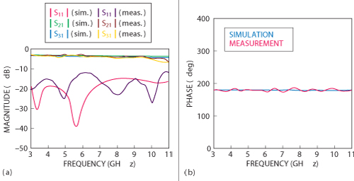
Figure 2 UWB balun simulation versus measurement. S-parameter magnitude (a); phase difference between balanced ports (b).
Balun Design and Verification
The UWB planar balun design is optimized with the help of 3D EM simulators. The simulated and measured results are shown in Figure 2. The physical dimensions after optimization (see Figure 1) are Ls=4.2 mm, Sc=0.1 mm, S=1mm, Rg=2.1 mm, R2=1.9 mm, R3=1.8 mm and R4=3.9 mm. The simulated results reveal that power is equally divided between the balanced ports, with an insertion loss of less than 0.6 dB and return loss of better than 14.5 dB over the 3 to 11 GHz band. The difference in phase and amplitude between the balanced ports is 180°±1.4° and 0.2 dB over the same band. Due to the microstrip-to-SCSL transition, return loss is better than reported by Bialkowski and Abbosh.4
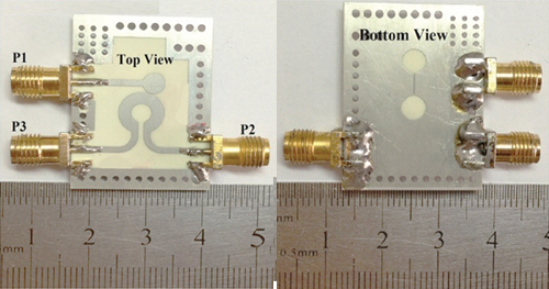
Figure 3 Fabricated UWB balun.
The balun is fabricated on a Rogers substrate with relative permittivity of 3.66, thickness of 0.508 mm, and loss tangent of 0.004 (see Figure 3). It is compact with dimensions of 0.5×0.4λg (where λg is the guided wavelength at the center frequency). For ease of measurement, the balanced ports are expanded with 50 Ω microstrip lines.
The S-parameters are measured using an HP8756A vector network analyzer employing the through-reflect-line (TRL) calibration technique. The balun is specified to operate from 3 to 11 GHz with a phase difference of the balanced ports equal to 180°±5°, an insertion loss less than 1 dB and a return loss greater than 11 dB. Slight differences between simulation and measurement are attributed to fabrication tolerances. Additional losses are due to connector loss, metal loss and radiation loss. Slight deterioration of insertion loss at the high end of the band is caused by radiation.
Implementation and Experimental Results
Figure 4 shows the assembled planar double balanced mixer (DBM) designed to operate over the UWB frequency range from 3.1 to 10.6 GHz. The individual components are combined in a harmonic balance simulator to optimize the mixer’s performance. Infineon silicon schottky cross-over ring diodes (BAT15-099R) are used. The internal crossover connections make it possible to access the quad from the LO and RF circuit without external crossovers, thus minimizing circuit parasitics. Identical baluns are used for the LO and RF, and their outputs are connected directly to the diode ring. The RF connection points to the quad are virtual grounds for the LO, and vice versa, assuring good LO/RF isolation. Unlike wound transformers, the baluns have no center ground connection that can be used as the IF. The usual technique of using a lone bonding wire interconnection for the IF is adopted so that its inductance effectively isolates the IF from the RF and LO (see Figure 4). The inductance of this interconnection, however, limits the IF bandwidth. Still, this is a simple, low cost, broadband approach.2
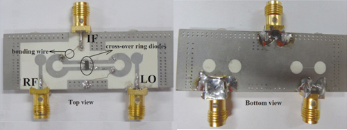
Figure 4 Fabricated UWB DBM.
The DBM is tested using an Agilent 8563EC spectrum analyzer calibrated with an E44198 power meter and E8257D signal generator. Losses of the probes and cables are measured separately and used to calibrate the measured results. Measured conversion loss versus LO power (RF power of -10 dBm) for the down-converter mode is shown in Figure 5. With the RF fixed at 8 GHz and the IF fixed at 100 and 50 MHz, a significant mixing effect at an LO drive level of 8 dBm is evident. For both IF frequencies, conversion loss is less than 11 dB at an LO power of 10 dBm.
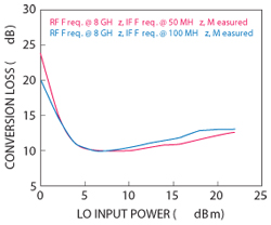
Figure 5 Measured conversion loss versus LO power level with an RF input power of –10 dBm.
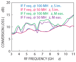
Figure 6 Measured conversion loss versus RF frequency (IF frequency = 100 MHz, 50 MHz).
Figure 6 plots the conversion loss at a 10 dBm LO drive level for a swept RF response from 3 to 11 GHz and IF frequencies of 50 and 100 MHz. The measured bandwidth is wider than the design goal. The conversion loss is 9 to 13 dB within the operating bandwidth of 3.1 to 10.6 GHz. This broadband performance is due to the high performance of the UWB balun. The simulated and measured conversion loss does not precisely match because it is not possible to realize the exact length and shape of the actual bonding wires in the simulation, as well as the additional unbalance caused by the bonding wires.
Measured and simulated port-to-port isolation of the DBM for the downconverter mode is shown in Figure 7. The bonding wire isolates both the RF and LO signals from the IF. The LO- and RF-to-IF isolations are greater than 25 and 40 dB, respectively, from 3 to 11 GHz. The LO-to-RF isolation is between 25 and 35 dB within the same swept range.
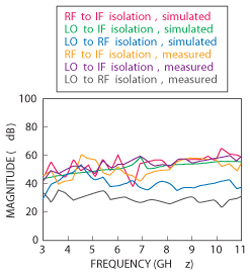
Figure 7 Simulated and measured LO/RF, LO/IF and RF/IF isolation as a function of RF frequency from 3 to 11 GHz.
Conclusion
Better performance is achieved in a UWB planar balun composed of microstrip lines, side coupled SCSLs and microstrip-to-SCSL transitions. A compact UWB double balance mixer based on this balun design exhibits a conversion less than 13 dB and high isolation among the three ports. It offers a high performance and cost-effective solution in a compact size for UWB applications.
References
- “Revision of Part 15 of the Commission’s Rules Regarding Ultra-Wideband Transmission Systems,” FCC, Washington, DC, Technical Report, ET-Docket 98-153, FCC02-48, adopted February 2002.
- S.A. Maas, Microwave Mixers,2nd edition, Artech House, Norwood, MA, 1993.
- Y.G. Kim, D.S. Woo, K.W. Kim and Y.K Cho, “A New Ultra-Wideband Microstrip-to-CPS Transition,” IEEE MTT-S International Microwave Symposium Digest, Honolulu, HI, June 2007, pp. 1563-1566.
- M.E. Bialkowski and A.M. Abbosh, “Design of a Compact UWB Out-of-Phase Power Divider,” IEEE Microwave and Wireless Components Letters, Vol. 17, No. 4, April 2007, pp. 289-291.
- M. Aikawa and H. Ogawa, “A New MIC Magic-T Using Coupled Slot Lines,” IEEE Transactions on Microwave Theory and Techniques, Vol. 28, No. 6, June 1980, pp. 523-528.
- J.B. Knorr, “Slot-Line Transitions,” IEEE Transactions on Microwave Theory and Techniques, Vol. 22, No. 5, May 1974, pp. 548-554.
- M.M. Zinieris, R. Sloan and L.E. Davis, “A Broadband Microstrip-to-Slot-Line Transition,” Microwave and Optical Technology Letters, Vol. 18, No. 5, August 1998, pp. 339-342.
- T. Itoh and R. Mittra, “Dispersion Characteristics of Slot Lines,” Electronics Letters, Vol. 7, No. 13, July 1971, pp. 364-365.