
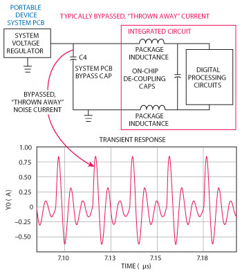
Figure 1 Reservoir current in typical bypass capacitors.
All electronic systems that use digital signal processing circuits (DSP) generate noise currents as an undesired byproduct of their function. These noise current impulses are too high in frequency for conventional regulators to supply directly, thus bypass capacitors are utilized in conjunction with system voltage regulators to supply these locally needed high frequency currents.
The added bypass capacitors also function to provide a local high frequency current reservoir for local logic, reducing supply voltage noise by bypassing the digitally generated, high frequency noise currents to system ground. This bypassing action shunts the high frequency noise currents away from the supply line, as shown in Figure 1, ultimately causing a “throw away” DC power drain (i.e., DC recharging of the bypass capacitors due to the losses in the system) on system power sources, batteries and capacitors.
Figure 1 shows typical reservoir current flowing (the “transient repsonse” waveform) as the result of active digital circuits and a typical system bypass cap (C4). Current spikes up to 1 A are shown. The “integrated circuit” in the figure can be any IC in any system that has some amount of digital activity on board. Power draw due to these digitally derived noise currents and losses can be greater than 50 percent of the total device and system power consumption. They are especially significant in portable devices, such as smart phones and portable computing devices, laptops and iPads, medical devices, ultra-low power systems powered by low capacity energy harvesting devices and the like. This form of digital power drain tends to increase as the device is utilized more heavily and application complexity increases in digitally driven systems.
To reduce this power drain, the conventional design wisdom is to use digital strategies in design so as to periodically deactivate power hungry digital circuits (some form of “burst mode” processing), minimize digital supply voltages, or “process shrink” the design to a lower gate length manufacturing process node. The strategies above can be thought of as power saving “defensive” actions, the designer striving to reduce switching circuit power drain as much as possible. Utilizing the above strategies generally requires some form of design rework on the digital circuits in order to accomplish the desired power reduction, which adds to time to market and cost.
It should be noted that no matter what “defensive” choices designers make in attempting to reduce digital power drain, a certain magnitude of “thrown away” current and power always remains when switching circuits are active. So long as designers use electron-based transistor devices in design, this type of energy waste will be present. This form of power drain can be thought of as a previously unknown energy source embedded in switching systems, considered unreachable and unusable, until now.
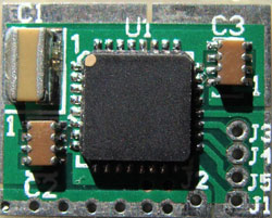
Figure 2 The CC-100 Power Optimizer.
A methodology and a design has been developed that can reduce the aforementioned digital power drain, tapping into this “hidden” source of wasted power, without the need for costly digital design rework. The methodology and design is intended to be an “add on” to existing digital and system designs, at the IC, PCB and system levels of integration. Targeting digital “thrown away” currents, the methodology and design intercepts and recycles these currents back into a given system. The implementation of the methodology is small and inexpensive enough to be integrated into existing ICs, PCBs and systems, drawing no operational power of its own.
Power Optimizer IC
The Power Optimizer IC (PowerOp) shown in Figure 2 (patent pending) is central to the real world realization of the mentioned methodology, a “proof of concept” device that fulfills the earlier mentioned needs and requirements. The IC functions to intercept “thrown away,” digitally generated currents, recycling them back into the system, reducing overall digital system power draw. This current recycling has been laboratory tested and shown to improve system battery life in portable devices by as much as 10 to 20 percent.
The “proof of concept,” production ready device, inserted in series with the ground side of a major system board bypass capacitor, has an ultra-low input impedance small enough so as not to interfere with the normal function of a PCB bypass capacitor. The output impedance of the device is high enough to force, with the inclusion of an appropriately sized return capacitor, “thrown away” currents back into the system.
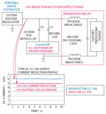
Figure 3 Typical application.
Figure 3 shows the same system as in Figure 1, only this time the device is inserted in series with the ground path of the system decoupling path and a current return cap (C3) is included for the device return path. The system bypass cap (C4) is the same cap as in Figure 1. The Power Optimizer IC, intercepting these “thrown away,” digitally generated noise currents, recycles previously wasted currents back into the system. This wasted current recycled (the “transient response” waveform in the Figure 1 case) is shown to improve system battery life (see current draw reduction — the “red” plot in Figure 3) in the system by as much as 10 percent.
Characterization data plots in Figure 4 for the device were taken utilizing a Wireless Telecom Group, JV9000 VCC noise generator, a Hewlett Packard 8860C signal generator, and a Hewlett Packard 8569B spectrum analyzer. The characterization data in Figure 4 was taken with a 50 Ω impedance matching resistor in series with the device “in” terminal and a switch connecting and disconnecting the “out” terminal from the generator side of the input 50 Ω impedance matching resistor. The 50 Ω resistor was included in the test set-up to facilitate test system impedance matching and is not needed for the device operation. All power data was taken for 10 consecutive seconds, averaged from the accumulated 10 raw data points, then averaged across various single frequency points across the 400 MHz to 1 GHz bandwidth of the CC-100 device output.
With the acquired Figure 4 power data, the rms current values and peak to peak voltage values were computed for each of the plots, allowing the gathered data to be related to the main device application shown in Figure 3. Where possible, the AC rms current values in the Figure 4 plots were checked against actual current measurements utilizing a super-cap powered, Digital Linear Feedback Shift Register (the “Digital Processing Circuits” referred to in Figures 1 and 3), that applied controlled, repeatable, pseudo-random induced VDD noise to the DUT. Currents were then computed by utilizing the equations Q = CV and Q/t = I, the test procedure designed to accurately measure the voltage discharge rate of the super caps in the test system. An Agilent AT-34411A data logging multi-meter was utilized to measure dc voltage values, Vi-Vf, while timing the discharge rate. The delta charge, Q = C(Vi-Vf) was then computed and divided by the elapsed time (Q/t = I). The test and analysis was done with the device in the test circuit and without the device (five times each, and averaged), the delta current and current/power savings computed.
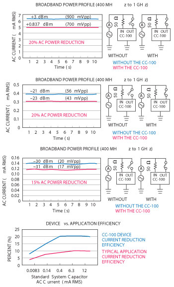
Figure 4 Power Optimizer characterization plots.
Correlation of Test Results
Correlation with a scaling factor of 0.5 was discovered to exist between the rms current data gathered for the device tests in the Figure 4 plots and the RMS current data (Figure 3) obtained with the super cap powered, pseudo random Digital Linear Feedback Shift Register, VDD noise generator applications test circuit. This 0.5 correlation factor was expected and is due to the varying nature and characteristics of the noise injected into the device. Symmetrical, random noise was injected in the device tests (the Figure 4 power plots), both voltage and current being allowed to vary. Non-symmetrical injected noise was injected in the application tests (Figure 3), with the voltage held constant by the regulator action in the system, thus allowing only the current to vary.
The device was found to respond differently to various types of injected noise. This delta in performance is graphically displayed in the last plot of Figure 4. What the data in Figures 3 and 4 means commercially, in terms of battery Watt-hours (Wh) is that this methodology and design effectively reduces the current load on portable device batteries, extending the effective time between needed battery recharges by up to 20 percent.
As an example, the DELL M5Y0X laptop battery, which is rated at 97 Wh, with this methodology and design being utilized, will cause the battery discharge rate to decrease and cause the system to operate as if the battery capacity was increased to 116 Wh. Systems utilizing Power Optimizer technology internally could be designed to fit a smaller form factor, since the battery capacity requirements are reduced, or handle more intense processing applications with the same performance in battery discharge rates.
The device has been packaged as shown in Figure 5 (patent pending) and used externally (no system re-design needed) in systems and devices with I/O ports like USB or Firewire in laptops, SDIO, or any portable device with port access to device internal power. The magnitude of the total power reduction utilizing the solution in this manner is dependent of I/O port activity, be it user mouse and keyboard activity or data transfers (SerDes) and such to and from the I/O port. Tests show a typical 10 to 20 percent battery life extension with an active USB I/O port with the Power Optmizer utilized in this fashion.
RF Power Integrity/Stability
A natural byproduct of the Power Optimizer current recycling is the device’s effect on power grid stability. System bypass capacitors, added to the system for impulse noise reduction, also function as AC terminations over frequency for system power grids. If the impedance of the system power grid and the impedance of the bypass caps in the system match over frequency, the power grid network will respond in a critically damped fashion over frequency to applied current impulses.
It is generally difficult, however, to obtain power grid-terminator matching over frequency, due to the tolerances and parasitics of and in the system components made commercially available for such systems. The S11 loss plots in Figure 6 graphically display this phenomenon. Figure 6a shows the wideband S11 of the device. With a series 50 Ω resistor placed at the input of the device, the overall VSWR of the device input is quite good, varying from nearly perfect, a VSWR of 1.0, to a worst case VSWR of 1.01. This plot shows that the low input impedance of the device is negligible to the total input resistance, and does not show much variation over the input bandwidth of the part. However, narrowband spectral peaks and dips remain in the Figure 6a plot, indicative of imperfections in the matching of the power grid on the device evaluation board, test system cabling and connectors.
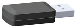
Figure 5 CC-100 embedded in a USB connector.
Compensating and optimizing for such mismatches in power grid and system impedances can lead to higher system component costs, longer design/optimization cycles and possible system design rework. What is desired is a methodology and design that can compensate for the under-damped mismatch effects created by the imperfections found in system components made available for system builds.
This methodology and design compensates for the aforementioned effects of component mismatches without the need for costly system design optimization/rework. Acting much like a negative feedback loop, the IC central to this methodology targets the “thrown away” currents that are the result of system transient activity, intercepting and recycling these “thrown away” currents back into the system, critically damping the power grid in a broadband fashion.
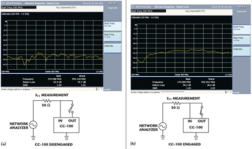
Figure 6 S11 with Power Optimizer disengaged (a) and engaged (b).
Figure 6b shows the S11 spectral results of the device’s negative feedback and power grid compensation. The Figure 6b plot demonstrates an increase in overall “returned” current (a 10 dB decrease in return loss, a slightly higher worst case VSWR of 1.03 vs. 1.01), but much reduced spectral peaks and dips, with respect to the Figure 6a plot. This return loss and VSWR decrease is not due to typical load mismatch effects, but is the result of Power Optimizer action, returning current to the system for reuse. Thus, in Figure 6b, the network analyzer power detectors show the device current return and negative feedback compensating for the imperfections present in the power grid on the Power Optimizer evaluation board, test system cabling, connectors, etc. This compensation aids in power reduction, transient suppression and overall power grid stability.
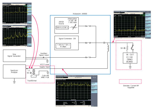
Figure 7 CC-100 test characterization setup with the JV9000.
A Walk Around the Loop
The Power Optimizer was designed to possess a broad spectral response to induced power line noise. Figure 7 is a Power Optimizer device test characterization setup that utilizes the capabilities of the Noisecom JV9000, a sine generator, a spectrum analyzer, an impedance matching transformer and the evaluation board. The device evaluation board is set up in such a manner so as to allow the device output to be engaged or disengaged from the test system for “with” or “without” the Power Optimizer.
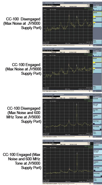
Figure 8 CC-100 DUT test results with the JV9000.
The JV9000 unit in the test system acts as a controllable, variable amplitude and frequency noise source that emulates the noise produced by digital switching activity in CMOS circuits. The unit possesses its own variable amplitude white noise source, carrier wave generator, inputs for an external sine wave generator, and a DC supply port.
In the device characterization set-up in Figure 7, the DC supply port is utilized as a signal monitor port, outputting the results of device performance to an impedance matching transformer, and the output of that is fed to a spectrum analyzer for analysis. The DC supply port on the JV9000 was designed for VCC biasing, not for signal monitoring, as the port is not impedance matched (see the S11 plot of the DC supply port in the lower middle of Figure 7) to a 50 Ω environment and attenuates the JV9000 output signal by roughly 30 dB. The impedance mismatch of the 50 Ω environment of the WBC1-1LB Coilcraft transformer to the unmatched DC supply port impedance creates reflective behavior (see Figure 7) between the output of the JV9000, the input of the device, and the input of the WBC1-1LB transformer. The reflective behavior of the JV9000 DC supply port; however, provides an excellent frequency domain test for the device’s capability of compensating, in a broadband fashion, power grid impedance mismatches.
In Figure 7, the frequency plot shown at the output of the JV9000 displays the spectral characteristics and frequencies applied to the device. The output signal, terminated into a 50 Ω input of a spectrum analyzer, shows a flat –19 dBm JV9000 maximum injected noise floor and a +2 dBm injected 600 MHz sine wave tone superimposed in the unit on the JV9000 output. Given the JV9000 spectrum applied to the output disengaged device, the two frequency plots at the end of the DC supply port and Coilcraft transformer shows the impedance mismatched, reflective spectrum fed to the spectrum analyzer, with and without the 600 MHz injected tone (upper left corner of Figure 7).
Power Optimizer Compensation Performance
Figure 8 (on page 84) shows the spectral results of the Power Optimizer with and without the device’s output engaged in the Figure 7 test system. The two disengaged plots show the spectrum seen at the spectrum analyzer input with the device disengaged. Peaking and reflection in the spectrum is observed, with major peaks in the noise only spectrum at 400 and 600 MHz at approximately –51 dBm levels, and the injected 600 MHz tone applied to the device at a –24 dBm level. The plots in Figure 8, with the device engaged, show reduced spectral peaking and reflection, the major peaks at 400 and 600 MHz at approximately –54 dBm, and the injected 600 MHz tone applied to the device reduced to –28 dBm.
Thus, a 3 to 4 dB reduction in spectral reflection and peaking is shown in the device, JV9000 driven tests, yielding a smoother, flatter spectrum, with the device compensating for system termination mismatches and consequent signal reflection on impedance mismatched nodes. The JV9000 tests correlate well to the S11 measurements taken and displayed in Figure 6, showing the Power Optimizer capability in compensating for system and power grid mismatches.
Conclusion
The Power Optimizer IC is central in the realization of system power reduction and power grid stabilization. A “proof of concept,” production ready device has been developed that saves system power and fulfills system power integrity needs and requirements. Due to the interception of “thrown away,” transient generated currents and consequent current mode recycling, the data presented shows that the IC damps the system power grid while reducing overall transient system power draw.
The implementation of the power reduction and power grid compensation methodology is process node and digital processing mode “agnostic,” in that it reduces overall digital system power up to 20 percent beyond what can be achieved by conventional power reduction methods alone, damping system power grids. It works in any process technology and in tandem with other power reduction and power integrity design/optimization efforts, and has been shown to be effective at all levels of system transient power draw.