

Characterization of dielectric properties, relative permittivity (εr, Dk, K), and dielectric loss tangent (Df, tan δ) are critical to RF design engineers. The parameter Dk drives characteristic impedance in transmission lines, coupling factors, and propagation velocity, so an accurate characterization is needed to avoid high magnitude reflections that cause poor power transfer through devices. Df is important for prediction of insertion loss in passive devices. If insertion loss is higher than predicted, then power transfer through a device may be too low and a higher power transmitter or more elements would be necessary. Presented here are four methods of extracting Dk and Df from dielectric samples of an unknown material and the pros and cons of each.
Split-Post Dielectric Resonator (SPDR)
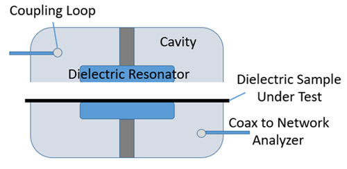
Figure 1. Split Post Dielectric Resonator Test
How it works:
A split-post dielectric resonator is a device used to measure the dielectric properties of relative permittivity and dielectric loss tangent. The SPDR fixture consists of an air cavity with two dielectric resonator pucks suspended in the cavity. A weakly coupled antenna loop to both ports 1 and 2 of a network analyzer excites the cavity, which is tuned to resonate at a specific frequency. There is a set gap between the dielectric resonators that can accept a dielectric sample in a sheet form. The introduction of this sample will cause the natural resonance of the resonators in the cavity to shift by some amount. This resonance shift can then be used to calculate the relative permittivity of the sample. The insertion loss between port 1 and 2 can also be measured before and after the insertion of the sample to calculate the loss tangent of the material.
Tolerances:
The tolerance of the Dk of the material under test is better than +/- 1% for an accurately machined and measured sample. The tolerance of the loss tangent is +/- 3% for accurate sample measurements and without consideration of thermal or cable-flex phase drifting in the measurement system. Since this portion of the measurement is based on phase angle, it is much more sensitive to small changes in the measurement system, so it is likely that larger tolerances in the loss tangent measurement are realistic. Repeating measurements and measuring multiple samples can help to drive this tolerance down. It is key to note that this measurement method measures the slab of dielectric material in the x-y plane.
When to use:
Most samples compatible with this style fixture are large (i.e. 10 cm) in the x and y directions and very short in the z direction (i.e. 1 mm). The microwave designer is interested in having the dielectric constant measured in the plane that is parallel to the highest electric field activity for their design in cases where the material is anisotropic, such as a material with a glass reinforcing weave. For this reason, this test method may not be suitable for a stripline design engineer using an anisotropic material. For isotropic materials, such as 3D printed, uniformly mixed loaded dielectrics, the measurement plane is not critical. For engineers interested in loss tangent only, the loss tangent in all planes typically matches for anisotropic materials as well as isotropic materials. This measurement technique is typically limited to frequencies of 10 GHz and below due to size limitations of the samples. Samples at higher frequencies need to be very thin and so the thickness tolerance of the samples becomes too great a percentage of the nominal thickness and electrical characterization becomes inaccurate.
Waveguide Resonant Cavity
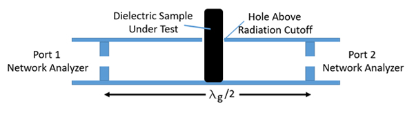
Figure 2. Waveguide Resonant Cavity Test
How it works
The waveguide resonant cavity method of Dk and Df extraction requires creating a matching iris leading in and out of the cavity at two ends of the waveguide. The iris spacing sets up a resonant mode in the cavity that will create a large suckout in transmission power in an S21 insertion loss measurement performed between the two ends of the waveguide with a network analyzer. A hole is created in the center of this resonant cavity in the center of the E-plane of the waveguide to accept a dielectric sample of a size that is below the cutoff for power radiation out of the waveguide. A dielectric rod of specific dimensions is inserted into the hole. This sample could be cylindrical or of rectangular prism shape, depending on what is easiest to manufacture a sample of very consistent thickness. If post-manufacture grinding is necessary to create this consistency, then a rectangular prism better lends itself to this process. Measuring the resonance of the S21 measurement and comparing it to the resonance absent of the sample is used to calculate the Dk of the sample. The specific volume of the sample is also used in this calculation and this volume measurement is the greatest source of uncertainty in the final Dk and Df values. The measurement in this case is relative to the plane of the sample that is parallel to the E-plane of the waveguide, so the long dimension of the dielectric rod. Similar to the SPDR method, this should be taken into account for anisotropic materials as pertaining to the electric field direction predicted for the component design.
Tolerances
The tolerance of the Dk of the sample measured using this method is < +/- 1% for a perfectly measured volume of sample and a sample with perfectly consistent dimensions top to bottom. This tolerance increases fairly rapidly as sample consistency and mechanical measurement accuracy decrease. The Df parameter can similarly be extracted using the volume of the inserted sample and the difference in S21 insertion loss value between the empty cavity and that which contains the sample. The tolerance of the Df parameter has not been published as could be found by the literature review for this document, but by similarity to the test method of SPDR, it is expected to be +/- 3 % for perfectly uniform and measured samples.
When to use:
This test method can be used up to any frequency for which a waveguide can be formed with a below cutoff frequency hole through it that will accept a dielectric rod that is possible to fabricate. At higher frequencies, this rod’s dimensions are smaller, so manufacturing tolerances and mechanical measurement tolerances create a higher percentage of uncertainty in the measurement. Practically speaking, this technique should be good through Ku-band frequencies, with potential to go higher with precision machining and measurement techniques. Higher order resonances can be used, but not above the operating cutoff frequency of the waveguide, which is a narrow band transmission medium.
Metallized Resonant Structures
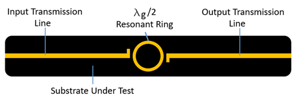
Figure 3. Edge-Coupled Ring Resonator Test
How it works:
One method of extracting Dk and Df properties from a metallized dielectric sample is to create a resonant structure with a metallic transmission line. This could be in the form of an end-coupled quarter-wave transmission line, an end-coupled ring resonator, or an edge-coupled ring resonator. This structure could be created in microstrip or stripline architecture. The basis of this measurement is that the resonator will be a quarter of a wavelength long at its self resonating frequency. A 2-port measurement can be taken of the connectorized or probe-launched metallized circuit using a network analyzer. The S21 response of this measurement will show a large resonance at the frequency corresponding to a quarter wave resonator as the lowest frequency resonance, with multiple higher frequency resonances at factors of wavelengths. The dielectric constant can then be back-calculated from the resonant frequency by finding the quarter wavelength of the frequency and extracting the Dk directly (in stripline) or through the effective Dk equation (in microstrip). Beyond the challenges faced in the pure dielectric measurement techniques (holding mechanical flatness in the sample and having accurate mechanical measurements) an additional challenge lies in the roughness of the metal creating the transmission line. The inward-facing roughness of the metal line creates an effect of making the resonator appear electrically to be longer than it is mechanically. It will measure a phase length longer than its mechanical length. So the effect of the metal roughness must be compensated for mathematically in the calculations or the tolerance of the measurements will become very large.
Tolerances
The tolerance of the measurement of metal roughness itself is certain to have an adverse effect on the final dielectric properties computations. Although 50 ohm linewidths prevent creating resonators much higher than 10 GHz in main resonance frequency, the re-resonant frequencies can be used to calculate the dielectric properties up to the limits of most measurement equipment.
When to use:
Examples have been shown of 5- and 10 GHz resonators being used for measurements up to 110 GHz.
Split-Cylinder Resonator (SCR)
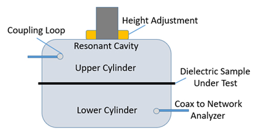
Figure 4. Split Cylinder Resonator Test;
How it works:
This test method utilizes a gold-plated cylindrical cavity with a split in the middle and an adjustable half to close the gap to zero for a pure cavity resonance method or to clamp the middle of the cylinder around a dielectric sample of prescribed thickness. This method works similarly to the split-post dielectric resonator method described in the first section, except that the cylindrical cavity is not limited by the resonance range of realizable sizes of dielectric resonators and so can be used to much higher frequencies than the complementary method. Conversely, the cylinder size would be difficult to realize for a fixture to measure dielectric properties below 10 GHz. Fixtures have been fabricated to measure Dk and Df up to 50 GHz, though the higher the measurement frequency for this method, the higher the measured property tolerance. This method utilizes coupling loops that are passed through small holes on coaxial lines through the walls of the cylindrical cavity. The cavity is excited to its natural resonance and the shift in resonance from the introduction of an unknown dielectric of known thickness is used to calculate the Dk of the material. Similarly, the change in insertion loss through the cavity with the introduction of the dielectric can be used to calculate the Df property.
Tolerances
Though tolerances of the Dk and Df parameters are not published for this structure, it is assumed that the Dk property tolerance is near the same +/- 1% as the the SPDR method at 10 GHz and climbs as the test frequency climbs, due to manufacturing tolerances in smaller cavities having a greater effect on the electrical tolerance.
When to use:
Fixtures have been fabricated to measure Dk and Df up to 50 GHz, though the higher the measurement frequency for this method, the higher the measured property tolerance.
Conclusions
After examination, there are reasons in favor and against using each of the different test methods above.
- Metallized circuit resonant structures have the disadvantage of having results skewed by the roughness of the inward-facing metal of the circuit, which is a difficult parameter to physically measure and compensate for. However, it may be worth attempting this compensation for anisotropic materials that will be used with electric fields in the z-axis such as a stripline design on a glass-reinforced dielectric sheet. This method would be the best to provide in-plane parameters relative to the proposed design.
- For isotropic materials, or for designs that utilize electric fields in the lateral plane, a pure dielectric measurement technique is typically better. Each of the three pure dielectric techniques (SPDR, Waveguide Cavity, SCR) has advantages depending on sample fabrication and target frequency.
- For frequencies over 10GHz, The choice between SCR and waveguide cavity techniques depend on sample size availability and electric field direction in the proposed design. But both methods have similar accuracy at these higher frequencies. The SPDR technique is at a disadvantage, as sample thicknesses become prohibitively thin.
- Outside of frequency range, the pure dielectric methods depend on sample preparation accuracy. If the material in question is available in sheets, then SPDR or SCR would be the best methods, due to the requirement to use a thin slab of material.
- If the material can be printed or molded into specific shapes, the waveguide cavity method has an advantage in that the volume of the larger dimensioned sample is more easily calculated, as a mechanical measurement tolerance of a larger dimension has less error percentage on that dimension. An additional advantage of the waveguide cavity method is that accurate dimensions of a smaller sample may be easier to hold.
References
https://www.qwed.com.pl/resonators_spdr.html
https://www.emlabs.jp/en/1-3-split.php
http://www.engineeringspecialties.net/
https://www.ipc.org/sites/default/files/test_methods_docs/2-5-5-13.pdf
https://www.ipc.org/sites/default/files/test_methods_docs/TM%202.5.5.14.pdf
https://www.emlabs.jp/en/1-10-rmethod.php
https://www.microwaves101.com/encyclopedias/dk-and-df-extraction-spreadsheet