

Some manufacturers of 5G systems are turning to higher levels of hardware integration and combining RF converters and baseband processing engines in system-on-chip (SoC) devices to address power consumption and board-space issues. While this integration has benefits, engineers tasked with characterizing these systems face new challenges accessing data because their once separate RF data converters are now combined with FPGAs and processors on the same chip.
Another confounding factor for engineers is the 5G standard itself. As a new standard, 5G is likely to evolve, so engineers will need to contend with not only changes in how to access data for characterization in an integrated device but also the potential for changes in reference waveforms and performance criteria. This places additional burdens on the characterization process, which needs to be flexible enough to deal with shifting requirements.
In order to deal with both data access through an SoC and with the potential of an evolving standard, an ideal characterization environment would need flexible signal generation and analysis capabilities capable of producing waveforms compliant not only with the current 5G standard but could also generate new waveforms as the standard evolves. This signal generation and analysis capability also needs to be able to extract RF data from new SoC hardware without requiring the RF engineer to be an expert in programming SoCs.
If this signal generation capability is contained in the same desktop environment as the signal capture and analysis capability, engineers could perform many RF test and characterization tasks without the need for traditional bench-top test equipment.
Virtual Test Equipment vs. Traditional Test Equipment
While there will always be a place for bench-top signal generators, spectrum analyzers, and other related traditional test equipment for certifying system performance, the cost and physical size of these instruments make them less desirable during the initial characterization and “what-if” phases of system design. Enabling algorithm developers, RF engineers, and system designers to access their own virtual testing “labs” can speed up design iterations and help get to the best designs faster.
Poor choices for hardware and algorithms can be weeded out early in the design process without having to tie up an expensive shared resource like bench-top test equipment, not to mention the associated testing staff who may own that equipment. Similarly, good design ideas can be identified quickly and developed to a higher degree before engaging in a more extensive testing process, greatly enhancing the likelihood of passing certification without extensive hardware rework and saving development time and cost.
The goal here is not to replace bench-top testing but to add software-based testing early in the process, reducing hardware prototype build costs and increasing engineering productivity.
But how can this type of desktop characterization environment be used with prototype hardware intended for 5G system development? Figure 1 shows the software-based characterization setup for an SoC device consisting of eight channels of RF ADCs and eight channels of RF DACs integrated with programmable logic and an MCU-based processing system.
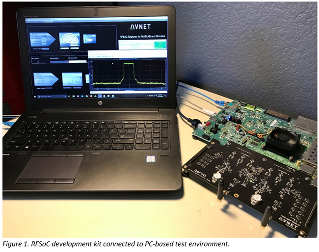
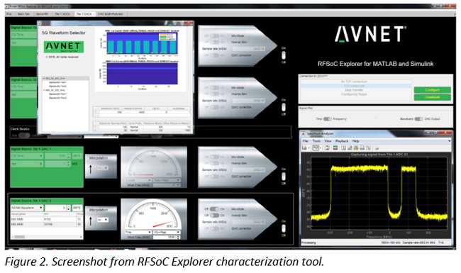
Signals will be generated on the PC from a MATLAB application and then sent into a Zynq UltraScale+ RFSoC device, out the device’s DACs, through the ADCs, and back to the PC. A PC-based application called RFSoC Explorer manages the data transfers, signal generation, and analysis functions as shown in Figure 2.
This “closed loop” testing mitigates the need for external test equipment and allows users to characterize the performance of the ADCs and DACs on the RFSoC to a level sufficient to make a go/no-go decision on the suitability of the hardware.
This software-based testing approach lets RF engineers access data converters embedded in an SoC without having to program the device themselves to enable data access and provides the flexibility required in signal generation that allows users to modify waveforms as necessary should the standards evolve.
Expanding the Testing Methodology
While a software-based testing methodology enables quick suitability decisions to be made, there are limitations, primarily the speed of the communications channel between the hardware and host computer and the speed of the testing software itself to do signal analysis. If the testing requirements require faster data rates for signal analysis, the same software front end can be used for signal generation, with traditional test equipment connected to the RFSoC outputs for data analysis. This method still allows for waveform programmability, while mitigating the effects of potential communications bottlenecks.
Additional test scenarios include using the programmable logic on the RFSoC device to act as its own signal generator or adding logic in the device to create its own test scenarios, like setting certain trigger conditions on incoming data and capturing only data of interest for further analysis on the PC, instead of streaming all data.