

High-quality copper foils and dielectric materials are important ingredients for high-performance, high reliability printed circuit boards (PCBs). While much has been covered in previous blogs about the dielectric material properties of PCBs, knowing more about copper can reveal how it impacts the performance of high frequency analog and high speed digital (HSD) PCBs. Not all PCB copper conductors are created equal.
Just as PCBs are produced with various dielectric materials, they can also be constructed with different thicknesses and types of copper. As detailed in the webinar from Rogers Corp., “Impact of Copper Properties on High Reliability, High Performance PCB Design,” the choice of copper grows more critical with increasing circuit frequency and speed. Specific copper characteristics can affect performance at millimeter-wave (mmWave) frequencies and in high speed digital (HSD) circuits. For example, the surface roughness of copper can affect a PCB’s insertion loss, phase consistency, and propagation delays. Copper surface roughness can yield electrical performance variations across one PCB as well as from PCB to PCB. Understanding the role of copper in high frequency, high speed circuits can ease the journey from computer models by leading to hardware that closely mirrors the models.
Circuit laminates feature dielectric insulators and copper conductors. A simple microstrip circuit includes a top layer transmission line and bottom layer ground plane, separated by a dielectric insulator layer. Several types of copper foils are available including electro-deposited (ED) copper and rolled copper. In an ED process, copper is plated onto a drum and the thickness of the copper sheets is determined by the rotating speed of the drum. The copper side against the drum has a smooth surface while the copper sheet on the outer side has a rougher surface. The copper grain structure runs perpendicular to the surface of the rotating drum. Rolled copper film is formed by an ingot of copper passed between a series of increasingly finer pressure rollers. The flexibility of the rolled copper can be enhanced via a heat-treating process called annealing; in which case it is known as rolled annealed (RA) copper. RA copper has both sides with typical surface smoothness of 0.35 µm RMS or better. ED copper has a smooth side against the drum and a rougher side on the outside of the drum. The smooth side is similar to that of RA copper, at about 0.35 to 0.40 µm RMS, but is smoother than the opposite side of an ED copper sheet.
That rougher side of an ED copper foil helps form a stable bond with dielectric substrates, stronger than the bond of rolled copper with the same substrates. With its crevices and valleys, that rough ED side forms a large effective bonding area for the dielectric material. It also lends itself to stronger wire bonds with ED copper than with RA copper. But ED copper lacks the malleability of rolled copper and is more prone to thermal cracks, especially during thermal cycling. Still, when etched to create transmission lines and circuit patterns, ED copper leaves smoother conductor sidewalls compared to rolled copper. The smooth sidewalls of etched ED copper conductors more closely reflect the models of circuit design computer simulation software, especially for the narrow conductors of high frequency/high speed circuits.
Measuring Roughness
Measuring the surface roughness of copper foils requires micrometer resolution, with surface roughness typically ranging from about 0.25 to 3.0 µm for different types of copper foils. Measurements can be made through physical contact, with a precision stylus or probe, although it must be capable of traveling along the surface peaks and valleys that define the roughness. Contact with a stylus can also cause damage to the copper surface. Alternately, noncontact measurements can be made through optical and laser-based microscopes. Such measurements provide high resolution but may not detect details hidden behind surface structures in the copper, such as where the foil has areas that form a mushroom shape. But as optical and laser microscopes improve their capabilities to perform three-dimensional (3D) measurements, they can better resolve the shapes of rough copper surfaces.
Measured copper surface roughness is determined according to specific parameters, such as Rz, the peak-to-valley measurement performed within a line, or Sz, the same surface roughness measurement, but done over an area. A future blog will take a closer look at the precision required for copper surface roughness measurements and the importance of the range of parameters that help define surface roughness.
Copper surface roughness affects the performance of mmWave and HSD circuits, especially as they move higher in frequency and speed. Increased surface roughness can affect conductor loss, signal phase, and propagation time. Conductor loss, along with dielectric loss, is part of a circuit’s insertion loss. It is measured for a given length of transmission line, such as microstrip or stripline, at a particular test frequency. Skin depth is the amount of the conductor being used by most of the RF current and as frequency increases, skin depth becomes thinner. At higher microwave or millimeter-wave frequencies, with very thin skin depth, any amount of copper surface roughness will contribute to conductor loss and impact phase angle and propagation velocity. Variations in the copper surface roughness will result in variations in insertion loss, phase angle, and propagation delay. Variations in copper surface roughness across multiple sheets of copper and multiple circuit laminates results in performance variations across lots of circuits produced with those materials, especially at higher frequencies such as in 5G small cells and 77 GHz automotive radars. Copper roughness variations tend to have greater effect on the signal plane than the ground plane even with the same roughness levels, especially as mmWave frequencies and HSD speeds increase. Increases in copper surface roughness cause increases in the effective dielectric constant (Dk) of a circuit, with resulting variations in transmission phase and propagation delays.
Thinner copper with smoother surfaces is important for mmWave and HSD circuit performance since thinner copper is more readily etched than thicker copper into the circuit features needed at high circuit frequencies and speeds. However, on thin laminates, such circuits can be affected by copper surface roughness and should be produced on laminates with low levels of copper surface roughness.
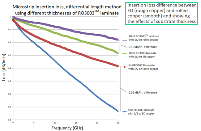
As an example of how copper surface roughness affects loss, RO3003™ laminates from Rogers Corp. (www.rogerscorp.com) were evaluated with microstrip test circuits using different types of copper and different substrate thicknesses. The thickest (20 mils) substrates yielded the lowest loss through 25 GHz using ½-oz. rolled copper with low copper surface roughness. The next-lowest loss occurred for ½-oz. ED copper with higher copper surface roughness. When the same two types of ½-oz. copper were used on thinner, 5-mil-thick substrates, loss rose dramatically, as normal when comparing circuits built on thin and thick substrates, with the highest loss for 5-mil-thick RO3003 laminates with ½-oz. ED copper. The results illustrated in the picture below, show that thin laminates with rough copper surfaces can be lossy, especially into the mmWave frequency range.
Attendees at the 2022 IEEE International Microwave Symposium (IMS) in Denver are invited to delve deeper into the impact of copper properties on PCB performance by joining John Coonrod at the MicroApps theater on Tuesday, June 21, 2022, at 1:30 p.m., for his presentation “An Overview of Copper Foil, How It’s Made, Roughness Effects, and RF/HSD Influences.” Copper is a vital component of circuit laminates and PCBs and knowing more about it can be especially helpful in mmWave applications such as 5G small cells and automotive radars.
Do you have a design or fabrication question? Rogers Corporation’s experts are available to help. Log in to the Rogers Technology Support Hub and “Ask an Engineer” today.
High-quality copper foils and dielectric materials are important ingredients for high-performance, high reliability printed circuit boards (PCBs). While much has been covered in previous blogs about the dielectric material properties of PCBs, knowing more about copper can reveal how it impacts the performance of high frequency analog and high speed digital (HSD) PCBs. Not all PCB copper conductors are created equal.
Just as PCBs are produced with various dielectric materials, they can also be constructed with different thicknesses and types of copper. As detailed in the webinar from Rogers Corp., “Impact of Copper Properties on High Reliability, High Performance PCB Design,” the choice of copper grows more critical with increasing circuit frequency and speed. Specific copper characteristics can affect performance at millimeter-wave (mmWave) frequencies and in high speed digital (HSD) circuits. For example, the surface roughness of copper can affect a PCB’s insertion loss, phase consistency, and propagation delays. Copper surface roughness can yield electrical performance variations across one PCB as well as from PCB to PCB. Understanding the role of copper in high frequency, high speed circuits can ease the journey from computer models by leading to hardware that closely mirrors the models.
Circuit laminates feature dielectric insulators and copper conductors. A simple microstrip circuit includes a top layer transmission line and bottom layer ground plane, separated by a dielectric insulator layer. Several types of copper foils are available including electro-deposited (ED) copper and rolled copper. In an ED process, copper is plated onto a drum and the thickness of the copper sheets is determined by the rotating speed of the drum. The copper side against the drum has a smooth surface while the copper sheet on the outer side has a rougher surface. The copper grain structure runs perpendicular to the surface of the rotating drum. Rolled copper film is formed by an ingot of copper passed between a series of increasingly finer pressure rollers. The flexibility of the rolled copper can be enhanced via a heat-treating process called annealing; in which case it is known as rolled annealed (RA) copper. RA copper has both sides with typical surface smoothness of 0.35 µm RMS or better. ED copper has a smooth side against the drum and a rougher side on the outside of the drum. The smooth side is similar to that of RA copper, at about 0.35 to 0.40 µm RMS, but is smoother than the opposite side of an ED copper sheet.
That rougher side of an ED copper foil helps form a stable bond with dielectric substrates, stronger than the bond of rolled copper with the same substrates. With its crevices and valleys, that rough ED side forms a large effective bonding area for the dielectric material. It also lends itself to stronger wire bonds with ED copper than with RA copper. But ED copper lacks the malleability of rolled copper and is more prone to thermal cracks, especially during thermal cycling. Still, when etched to create transmission lines and circuit patterns, ED copper leaves smoother conductor sidewalls compared to rolled copper. The smooth sidewalls of etched ED copper conductors more closely reflect the models of circuit design computer simulation software, especially for the narrow conductors of high frequency/high speed circuits.
Measuring Roughness
Measuring the surface roughness of copper foils requires micrometer resolution, with surface roughness typically ranging from about 0.25 to 3.0 µm for different types of copper foils. Measurements can be made through physical contact, with a precision stylus or probe, although it must be capable of traveling along the surface peaks and valleys that define the roughness. Contact with a stylus can also cause damage to the copper surface. Alternately, noncontact measurements can be made through optical and laser-based microscopes. Such measurements provide high resolution but may not detect details hidden behind surface structures in the copper, such as where the foil has areas that form a mushroom shape. But as optical and laser microscopes improve their capabilities to perform three-dimensional (3D) measurements, they can better resolve the shapes of rough copper surfaces.
Measured copper surface roughness is determined according to specific parameters, such as Rz, the peak-to-valley measurement performed within a line, or Sz, the same surface roughness measurement, but done over an area. A future blog will take a closer look at the precision required for copper surface roughness measurements and the importance of the range of parameters that help define surface roughness.
Copper surface roughness affects the performance of mmWave and HSD circuits, especially as they move higher in frequency and speed. Increased surface roughness can affect conductor loss, signal phase, and propagation time. Conductor loss, along with dielectric loss, is part of a circuit’s insertion loss. It is measured for a given length of transmission line, such as microstrip or stripline, at a particular test frequency. Skin depth is the amount of the conductor being used by most of the RF current and as frequency increases, skin depth becomes thinner. At higher microwave or millimeter-wave frequencies, with very thin skin depth, any amount of copper surface roughness will contribute to conductor loss and impact phase angle and propagation velocity. Variations in the copper surface roughness will result in variations in insertion loss, phase angle, and propagation delay. Variations in copper surface roughness across multiple sheets of copper and multiple circuit laminates results in performance variations across lots of circuits produced with those materials, especially at higher frequencies such as in 5G small cells and 77 GHz automotive radars. Copper roughness variations tend to have greater effect on the signal plane than the ground plane even with the same roughness levels, especially as mmWave frequencies and HSD speeds increase. Increases in copper surface roughness cause increases in the effective dielectric constant (Dk) of a circuit, with resulting variations in transmission phase and propagation delays.
Thinner copper with smoother surfaces is important for mmWave and HSD circuit performance since thinner copper is more readily etched than thicker copper into the circuit features needed at high circuit frequencies and speeds. However, on thin laminates, such circuits can be affected by copper surface roughness and should be produced on laminates with low levels of copper surface roughness.
As an example of how copper surface roughness affects loss, RO3003™ laminates from Rogers Corp. (www.rogerscorp.com) were evaluated with microstrip test circuits using different types of copper and different substrate thicknesses. The thickest (20 mils) substrates yielded the lowest loss through 25 GHz using ½-oz. rolled copper with low copper surface roughness. The next-lowest loss occurred for ½-oz. ED copper with higher copper surface roughness. When the same two types of ½-oz. copper were used on thinner, 5-mil-thick substrates, loss rose dramatically, as normal when comparing circuits built on thin and thick substrates, with the highest loss for 5-mil-thick RO3003 laminates with ½-oz. ED copper. The results illustrated in the picture below, show that thin laminates with rough copper surfaces can be lossy, especially into the mmWave frequency range.
Attendees at the 2022 IEEE International Microwave Symposium (IMS) in Denver are invited to delve deeper into the impact of copper properties on PCB performance by joining John Coonrod at the MicroApps theater on Tuesday, June 21, 2022, at 1:30 p.m., for his presentation “An Overview of Copper Foil, How It’s Made, Roughness Effects, and RF/HSD Influences.” Copper is a vital component of circuit laminates and PCBs and knowing more about it can be especially helpful in mmWave applications such as 5G small cells and automotive radars.
Do you have a design or fabrication question? Rogers Corporation’s experts are available to help. Log in to the Rogers Technology Support Hub and “Ask an Engineer” today.