

High-frequency circuit designers must often consider the performance limits, physical dimensions, and even the power levels of a particular design when deciding upon an optimum printed-circuit-board (PCB) material for that design. But the choice of transmission-line technology, such as microstrip or grounded coplanar waveguide (GCPW) circuitry, can also influence the final performance expected from a design. Many designers may be familiar with the stark differences between high-frequency microstrip and stripline circuitry. But GCPW circuitry, while also having its differences from traditional microstrip, also offers many benefits for high-frequency circuit designers to consider. In making the choice, it can help to understand just what different types of PCB material can have on the microstrip and GCPW circuits. The differences between the two structures can be seen in the following simple illustration.
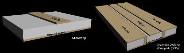
As a quick comparison, microstrip circuitry features a signal conductor fabricated on top of a dielectric layer, with a conductive metal ground plane on the bottom of the dielectric material. GCPW achieves an extra level of grounding and isolation by fabricating a signal conductor in between two ground conductors, all on the top of a dielectric layer, with an additional ground plane on the bottom of the dielectric layer. Conductive-metal-filled viaholes connect the top-layer and bottom-layer ground planes for consistent ground performance. In addition, many GCPW circuits employ ground straps to provide electrical connections for the two top-layer ground conductors for consistency around circuit discontinuities, such as junctions.
As different as the two circuit approaches may appear, the tight spacing of the top-layer grounds and signal conductor for the GCPW approach enables it to achieve low impedances and to tune the impedance by adjusting the spacing between the grounds and the signal line. The impedance increases as the spacing between the top-level ground conductors and the signal conductor increases. In fact, as the spacing of a GCPW circuit’s top-layer grounds from the signal conductor increase, those grounds have less effect on the circuit and a GCPW circuit with enough spacing between the top-layer grounds and the signal conductor electrical resembles a microstrip circuit.
Why use one transmission-line approach over the other? Obviously, microstrip has an “elegant simplicity” to it, which makes it easier to fabricate and even easier to model via computer than GCPW circuits. With their strong ground structure, GCPW circuits are capable of lower-loss performance at much higher frequencies than microstrip circuits, and offer great potential for designs working well into the millimeter-wave frequency range, even to frequencies of 100 GHz and beyond. Microstrip which, with stripline, is one of the most popular transmission-line formats at microwave frequencies, suffers increased circuit losses into the millimeter-wave frequency range, making the circuit technology less efficient for use at frequencies of 30 GHz and beyond.
What roles do PCB materials play in the choice of using microstrip or GCPW transmission-line approaches? Such material parameters as dielectric constant (Dk) and consistency of Dk through the material will impact the electrical performance of either transmission-line approach. The manner in which the electromagnetic (EM) fields travel through each circuit structure will have a great deal to do with the effective Dk that is exhibited for a particular circuit material, since those EM fields can flow within the dielectric material and outside of the dielectric material. In microstrip circuits, for example, with their top-side transmission lines and bottom-side ground planes, the EM fields are contained mainly within the dielectric material between the two metal planes, with a high field concentration at the edges of the signal conductor. For microstrip circuits, the effective dielectric constant is closely related to the specified Dk of the PCB material, such as RO4350B™ PCB material from Rogers Corp. (www.rogerscorp.com), which has a process specification of 3.48 in the z direction (thickness) at 10 GHz. The material’s Dk is held to impressive ±0.05 tolerance across the material.
The effective Dk of a PCB material will essentially determine the size of circuit structures required to achieve a specific characteristic impedance, such as 50 ?. So, for microstrip transmission lines on, for example, RO4350B circuit material, circuit width for 50 ? will be based on a Dk of 3.48. But for GCPW using the same material, because the circuit’s effective Dk is reduced because more of the EM field is in the air above the circuit rather than in the PCB dielectric material, the effective Dk is lower when compared to microstrip. The difference in effective Dk for GCPW and microstrip depends on the thickness of the substrate used by the GCPW circuitry and the spacing between the ground-signal-ground conductors on the top layer.
PCB fabrication issues have less impact on microstrip circuits than GCPW circuits. For example, PCB copper plating thickness variations have little effect on the performance of microstrip circuits but they can impact the performance of GCPW circuits. Thicker copper plating on PCBs for microstrip circuits can slightly reduce the insertion loss and lower the effective Dk of the circuit. For GCPW circuits, PCBs with thicker copper plating lead to an increase in the EM fields between the top-layer ground, signal, and ground field paths, with more of the EM fields in the air above the GCPW circuit. With more of the fields in the air above the circuit, signal losses decrease and the effective Dk of the PCB decreases for a GCPW circuit, all because of thicker PCB copper plating thickness.
As a quick comparison, microstrip supports moderate-bandwidth circuits through microwave frequencies, although with high radiation loss at higher, millimeter-wave frequencies and difficulty at achieving mode suppression at millimeter-wave frequencies. Microstrip circuits suffer minimal sensitivity to PCB fabrication techniques and material characteristics, such as copper plating thickness and copper thickness variations. In contrast, GPCW suffer only moderate radiation loss at millimeter-wave frequencies, and are capable of moderate or better mode suppression at millimeter-wave frequencies, making this circuit technology a strong candidate for designs at 30 GHz and higher. In addition, GCPW circuits are only moderately sensitive to PCB fabricate techniques and variations, making them well suited for production-volume applications at higher frequencies.
To learn more about the differences of microstrip and GCPW circuits and the PCB materials that suit them for different applications, those attending the 2015 IEEE International Microwave Symposium (IMS) this coming May 17-22, 2015 in Phoenix, AZ (www.ims2015.org) can attend the Microwave Application Seminars (MicroApps) presentation by John Coonrod of Rogers Corp., “Microwave PCB Structure Selection: Microstrip vs. Grounded Coplanar Waveguide,” scheduled for Tuesday, May 19, 2015.
Do you have a design or fabrication question? Rogers Corporation’s experts are available to help. Log in to the Rogers Technology Support Hub and “Ask an Engineer” today.